My notes:
Field-programmable gateway array, an integrated circuit consisting of an array of programmable logic blocks with programmable routing between the blocks that allows the device to be configured after manufacturing to perform complex digital logic functions.
The configuration is generally specified using a hardware description language (HDL).
1956, the first programmable logic device (PLD) was invented. PROM, Programmable Read only Memory. Commercially available in 1969. Fixed AND plane, the address decoding logic. Programmable OR plane through the change of memory contents.
1971, Erasable Programmable Read-only Memory (EPROM).
1975, Programmable Logic Arrays (PLAs).
1978, Programmable Array Logic (PALs). OR plane fixed, AND plane programmable.
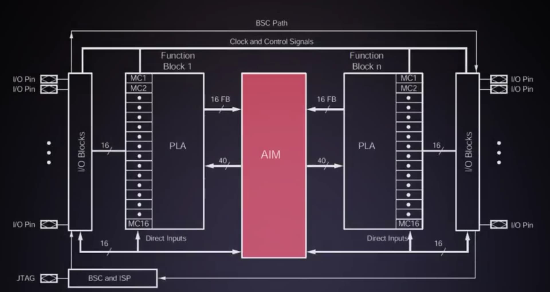
Complex Programmable Logic Device (CPLDs), multiple PALs in the same package with registered outputs and an interconnecting programmable fabric.
1980, Naval Surface Warfare Center developed a computer with 600000 reprogrammable gates.
1984, Altera EP300 with a quartz window to shine an ultraviolet lamp to erase the EPROM cells.
1985, Xilinx XC2064, first commercially viable FPGA. Programmable gates and programmable interconnects. 64 Configurable Logic Blocks, each with 3-input lookup tables (LUTS).
FPGAs consist of a wire, a gate, and a register or flip-flop. The chip is made of an array of flip-flops with wires that can connect them together in patterns that create the logic for larger functions, like counters, timers, state machines, arithmetic logic units, and CPUs.
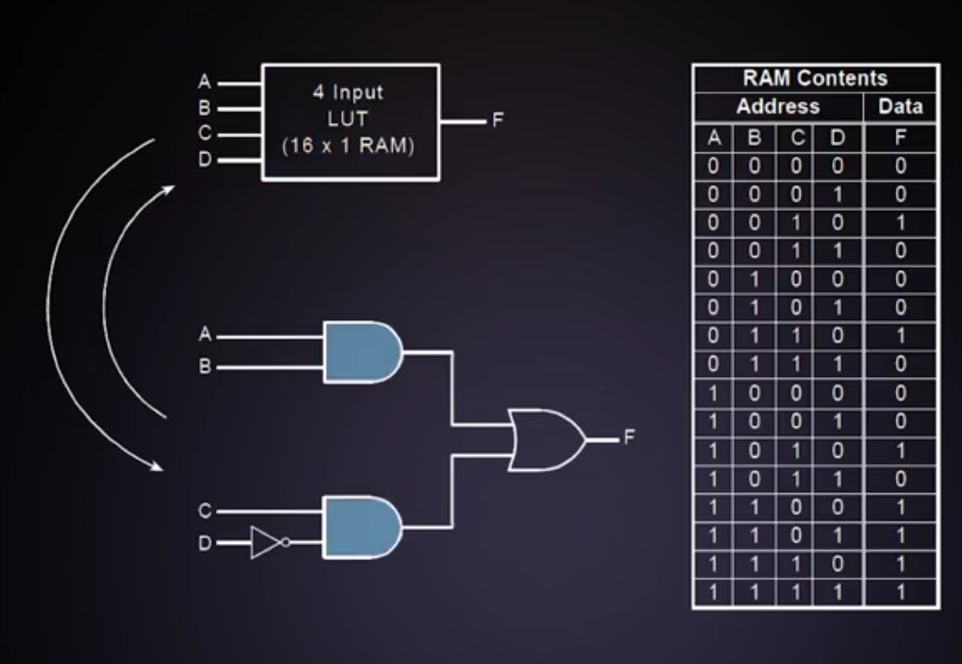
The logic is implemented in memory, in lookup tables.
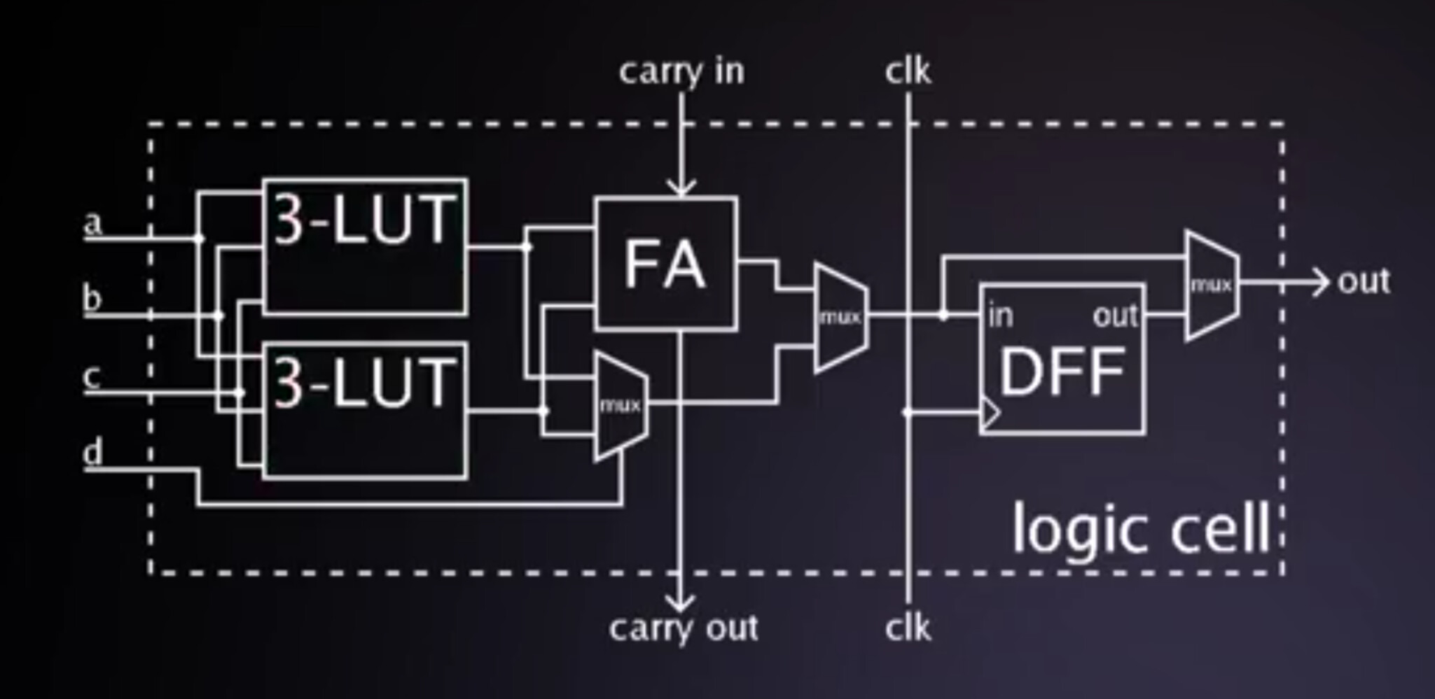
An FPGA logic cell consists of a 4-input LUT, a Full Adder (FA) and a D-type Flip-Flop. In normal mode the two LUTs are combined via a mux. In Arithmethic Mode the outputs are fed to the FA.
The user can determine the function of small clusters of gates, the logic cell, and how that cluster is connected to other clusters on the chip, gradually building up a circuit by connecting logic cells. Global routing networks for clock signals.
Configuration memory:
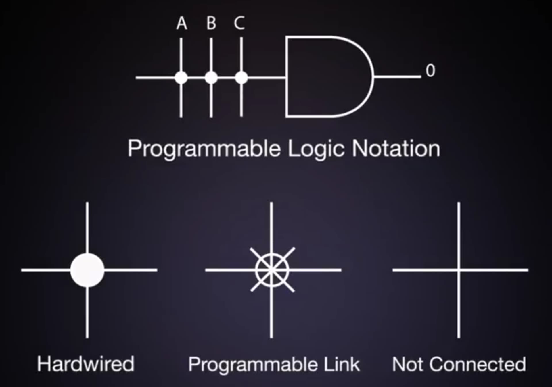
- antifuse are highly reliable, but one time programmable and expensive.
- flash are highly reliable, reprogrammable, more expensive than SRAM.
- SRAM are reprogrammable and have the highest density and lowest cost.
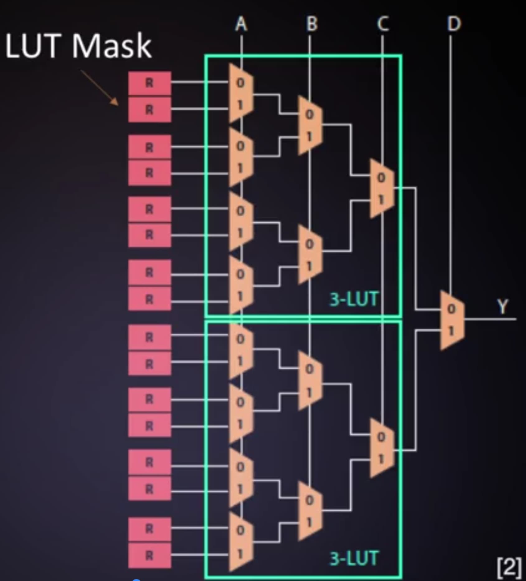
A LUT is tipically built out of SRAM bits to hold the configuration memory, a LUT mask and a set of multiplexerst to select the bit of the SRAM that drives the output.
Larger LUTs can create more logic and require less routing. Smaller LUTs require more routing and offer better efficiency.
FPGA Design
- Design entry, schematic or HDL
- Functional simulation
- Synthesis or mapping: check the design for errors, build a database, synthesize and optimize, map the design to device resources.
- Place and route or fitting:
- Simulation: static timing analysis can determine if there are violations of clock requirements.
- Programming
- Test and integration
- Release
Quartus Prime is a tool from Altera that allows schematic capture, import of IP blocks, HDL text entry in VHDL, Verilog and System Verilog, state machine entry and import EDIF files. Allows fitting balanced, high performance for speed, low power or small area.
Timing Analysis
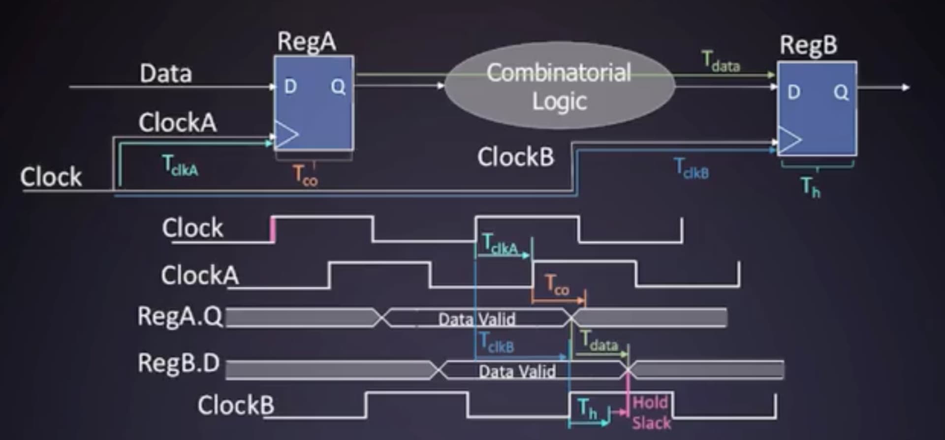
Clocks provide synchronization for error-free transfer. During the transition from one value to another, the value will be incorrect. We need to wait until the data is stable before using it. Data must be stable before and after the clock edge synchronization signal to be reliably transferred.
Launch edge activates the source register in a register-to-register path.
Latch edge activates the destination register and captures the data.
Setup time is the minimum time the data signal must be stable before the clock edge.
Hold time is the minimum time the data signal must be stable after the clock edge.
Compare the time when the data arrives with the time that the clock arrives to see if there is a setup violation.
Timing closure: when all timing requirements are met.
Timing violations can occur when data path is too long, the requirements too short, clock skew, etc.
FPGA architectures
Amount of logic is measured by system gates, logic elements, slices, macrocells, LABs, ALMs, etc. The cost per gate is important. Also speed, measured by maximum clock frequency. In opposition to speed is low power consumption. Deterministic timing is important. Some are not reprogrammable. Reliability is a major concern. Some have hard ip available on chip for memory, DSP blocks, transceivers, etc. Endurance of data retention.
Xilinx CPLD
Efficient in the implementation of comparators and decoders, not efficient in adders or shift registers.
XC9500XL family
- Deterministic timing: 5 nanoseconts pin-to-pin logic delays
- 5V I/O.
- Flash cells for routing, reprogrammable.
- 20 years of data retention.
- 10000 program/erase cycles endurance.
- 288 macrocells, 6400 gates, 288 flip-flops.
- Clock at 208 MHz.
- I/O rich device, unlike an FPGA.
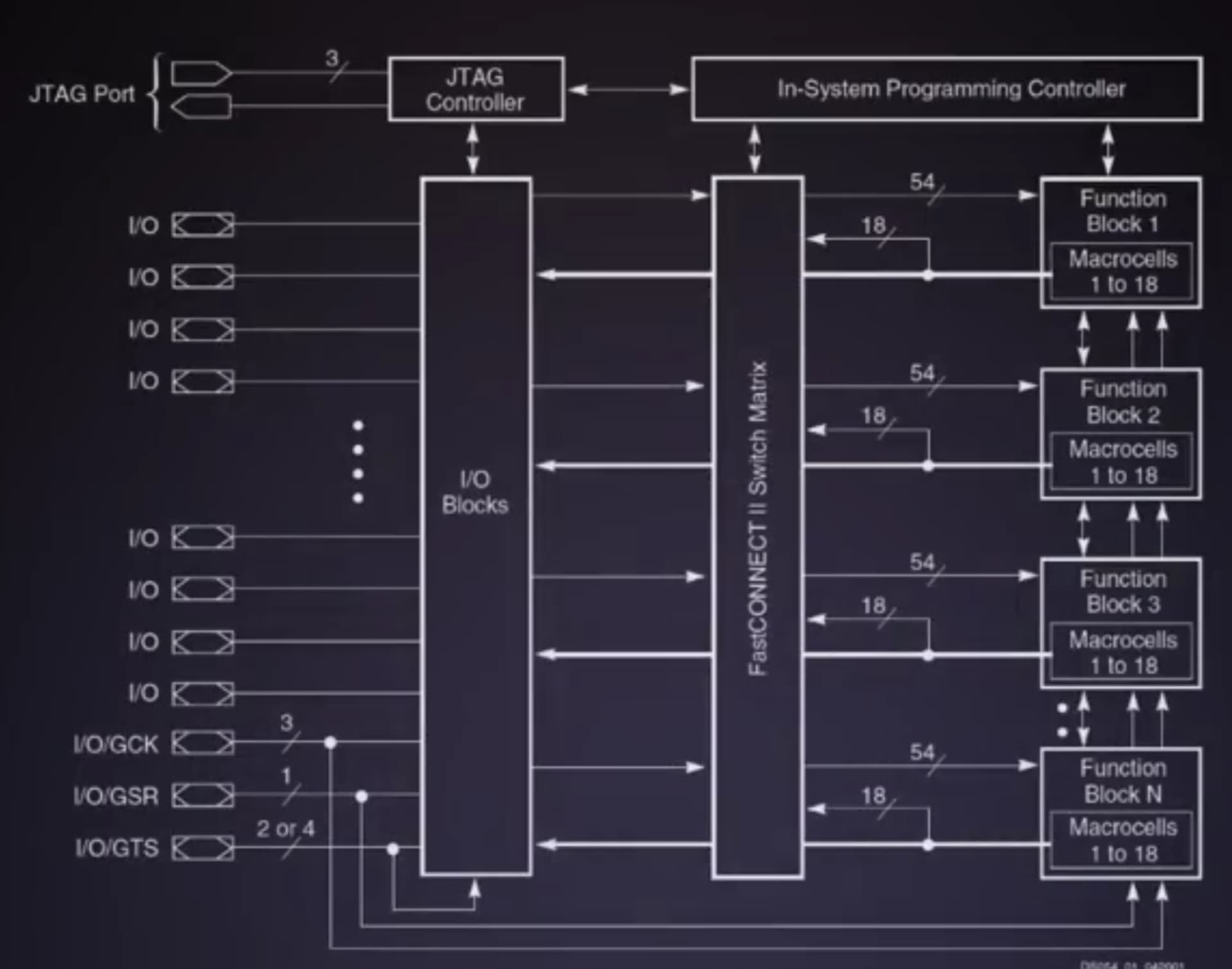
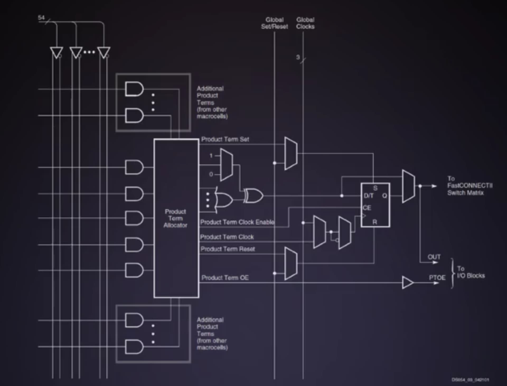
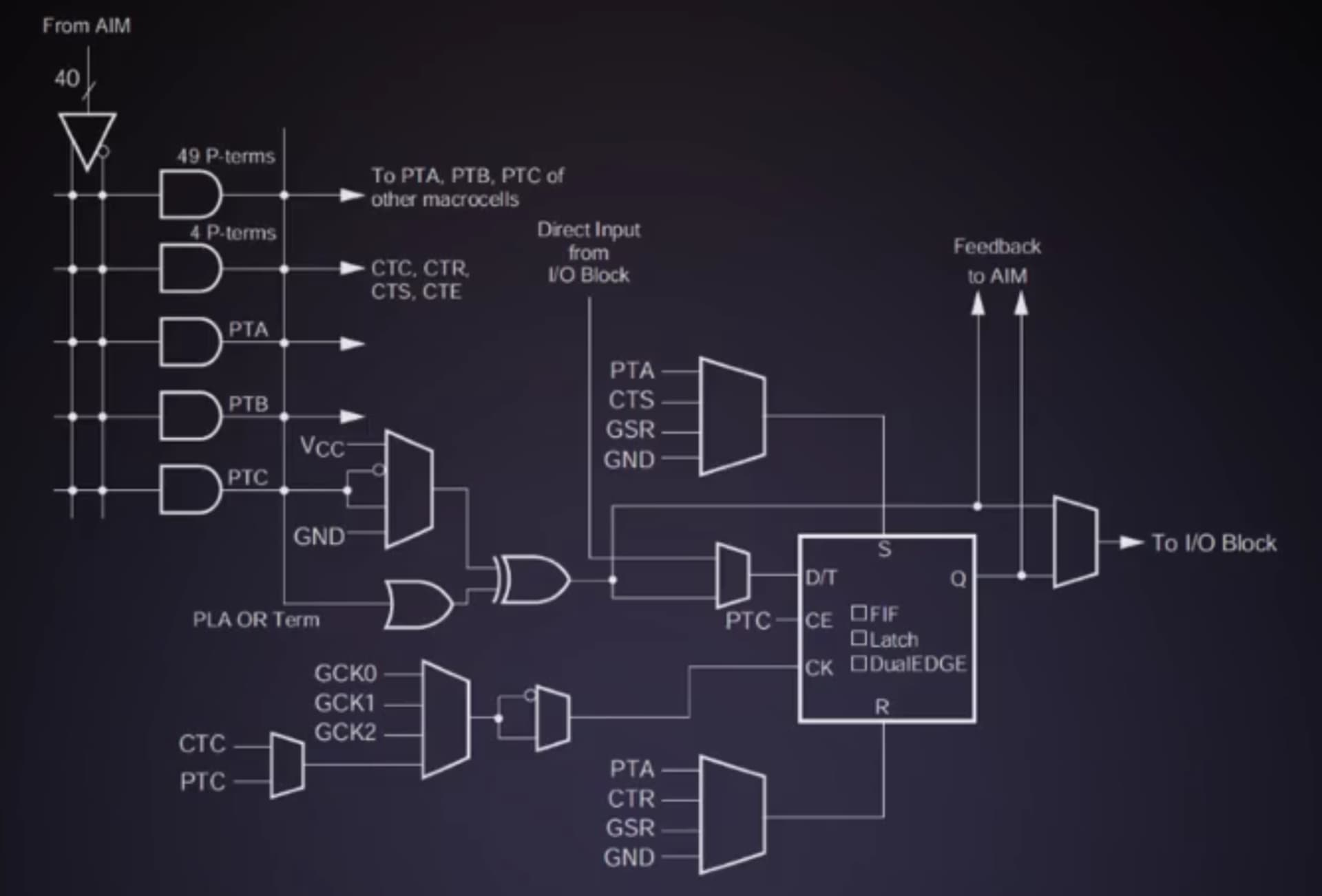
The macrocell can AND up to 54 signals, and then OR together 5 of these plus 5 from an adjacent macrocell.
Coolrunner II
- 1.5 V to 3.3 V
- 512 macrocells
- 270 I/O
- Deterministic timing: 5 nanoseconts pin-to-pin logic delays
- 323 MHz
- Non-volatile data transferred to SRAM cells for routing, reprogrammable
- 1000 program/erase cycles
- 20 year data retention
The macrocell can AND up to 40 signals and then or together 5 of these. Feed forward from other macrocells is through the AND array.
Xilinx small FPGAs
Xilinx Spartan 3AN
- Reprogrammable flash configuration
- 1400K system gates
- 25344 logic cells
- 350 MHz
- 502 I/O pins
- 20 years data retention
- 100K program/erase cycles
- Security through integration of internal configuration and memory on a single chip
- IP blocks for RAM, multipliers, and digital clock managers
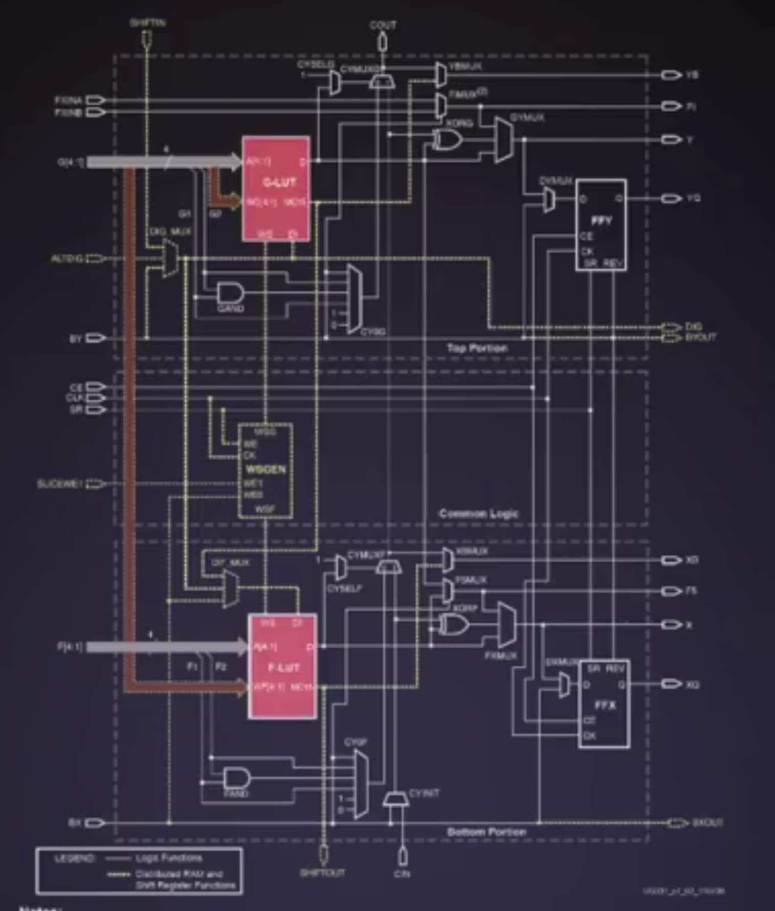
A slice has 2 4-input LUTs and 2 flip-flop outputs, plus some carry chain logic and shift-clock generation.
Spartan 6 FPGA
Requires external flash memory to load the configuration at power up. A delay of several milliseconds before the device becomes active.
- 147443 logic cells
- IP: 180 DSP slices, 4824 of RAM, 8 high speed transceivers.
- 540 I/O pins
- 400 MHz
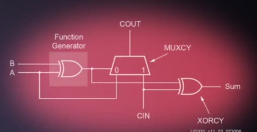
1 adder bit per LUT with carry lookahead and dedicated MUXCY and XORCY.
Xilinx Larage FPGAs
Artix-7
- Reprogrammable SRAM configuration which requires external memory to load the configuration
- 215360 logic cells, enough for a 32 bit CPU.
- 628 MHz clock
- 1412 MHz toggle frequency
- 500 I/O pins
- IP: RAM, clock management titles, DSP slices, analog to digital converter