# FRP-52: Trusted SILOs: Side-channel Isolated Logic Oases
**URL:** https://collective.flashbots.net/t/frp-52-trusted-silos-side-channel-isolated-logic-oases/5896
**Category:** FRPs - Flashbots Research Proposals
**Tags:** hardware
**Created:** [August 7, 2026, 4:23pm UTC](https://collective.flashbots.net/t/frp-52-trusted-silos-side-channel-isolated-logic-oases/5896 "2026-08-07T16:23:29Z")
**Posts on this page:** 3
**Page:** 1
### Author:  [@ernwa](https://collective.flashbots.net/u/ernwa)
#### Post date: [August 7, 2026, 4:23pm UTC](https://collective.flashbots.net/t/frp-52-trusted-silos-side-channel-isolated-logic-oases/5896/1 "2026-08-07T16:23:29Z")
| id | 52 |
| --- | --- |
| title | Trusted SILOs: Side-channel Isolated Logic Oases |
| team | Andrea Waite & ml\_sudo |
| created | 2025-07-09 |
| status | completed |
# Trusted SILOs: Side-channel Isolated Logic Oases
Trusted Execution Environments (TEEs) and other secure ICs like offline wallets and smart cards provide isolated enclaves to protect code and data from compromise of any system connected to them. This makes the designers of TEEs responsible for the one basket users’ increasingly valuable secrets are kept in. Adoption of cryptocurrency, AI hack tools, and increasingly invasive surveillance raises individuals’ value at risk and the chance of being a target.
We expect a boom of companies releasing new secure ASICs, and for these entrants to face an unprecedented deluge of hardware-level _side-channel analysis_ and _fault injection attacks_ . Current mitigation techniques exist to address these attacks, especially at the logic level, and there are research groups actively working to secure power distribution networks, but such techniques are generally reported as “proofs of concept” in academic papers, requiring a specialized security-focused analog IC design skillset to implement.
This report presents a synopsis of upcoming attacks and a menu of best-in-class, synergistic countermeasures to integrate into most ASIC design flows for non-specialist designers on tight timelines. Special attention is paid to higher level concerns like modularity, defense-in-depth, and (area-delay-power) efficiency.
pdf located on my github:
> **[FRP-52%20-%20Trusted%20SILOs%20--%20Side-channel%20Isolated%20Logic%20Oases.pdf](https://github.com/ernwa/SILOs/blob/main/FRP-52%20-%20Trusted%20SILOs%20--%20Side-channel%20Isolated%20Logic%20Oases.pdf)**
* * *
in markdown:
# Side-channel Isolated Logic Oases
# Hardening ICs Made Easy
by Andrea Waite + ml\_sudo
### Introduction
Trusted Execution Environments (TEEs) – Intel SGX/TDX, Arm TrustZone, and AMD SEV, for example – provide isolated enclaves intended to protect code and data even if the operating system or hypervisor is compromised. This makes the designers of TEEs responsible for the one basket in which all valuable secrets are kept. Increasing ubiquity of cryptocurrency, AI tools, and surveillance raises both the value at risk and the chance of being a target. We expect a boom in the design of new TEE and other secure ASIC hardware, and for these new entrants to face an unprecedented deluge of hardware-level _side-channel analysis_ and _fault injection attacks_.
This report presents a synopsis of upcoming attacks and a menu of synergistic countermeasures that can be efficiently integrated into most ASIC design flows for those thrust into this new Wild West. Side-channel attacks exploit unintentional information leakage (e.g. power consumption, electromagnetic emission, timing) to infer secrets, while glitch attacks actively induce faults (e.g. by momentarily disturbing voltage or clock) to bypass security checks or obtain incorrect computations. While always a concern for military and high-level encryption hardware, traditional industry threat models for TEEs have have deprioritized hardware-level attacks compared to software hacks.
This gap is now a dangerous open manhole: Cryptocurrency has created a buffet of instant profit potential. Open-source hardware platforms like ChipWhisperer and signal-processing algorithms are continuously reducing the time, money, and expertise needed to mount potent attacks. Simultaneously, increasing chip complexity and use of opaque IP cores are expanding the attack surface for adversaries to remotely exploit hardware-level side channels, compromising TEE guarantees without chip tampering or even physical presence.
### Know the Enemy and Know Yourself
> “By holding our forces in an unassailable position, we deny battle outright and force the enemy into other avenues of decision.”
> -- Carl Von Clausewitz, _On War_
From an attacker’s point of view, hardware-level attacks are one toolkit hanging on a shelf with many other tools. For a defender to know whether and which hardware attacks they should prepare for, they must know their enemy's goals and incentives. We believe that for the majority of commercial TEE makers, the enemy is not a hacker looking for a Defcon talk or a gamer trying to run Linux on their gaming console; it is an organized enterprise, government or criminal, seeking to maximize their _expected utility_ – return on investment under exposure risk.
This perspective immediately suggests that defense must also be economically rational. Defenders are faced with their own tradeoffs -- NRE costs, development cycle time, designer skill, tooling availability, required performance envelopes -- and thus usually don't get enough time or money to do a perfect job. They must allocate their defense resources for wide, overlapping, synergistic coverage across multiple domains, starting with the most vulnerable.
As Clausewitz points out, a rational attacker finding a Maginot Line will attack instead through Ardennes Forest. To dissuade attack altogether means allocating assets both broadly and in depth: overlapping layers of fortification, detection, and deterrence. No one layer can or should be overbuilt at the expense of breadth or depth. The example of the Maginot line is instructive: it performed as intended as a total deterrent but only for the ground it defended, at the opportunity cost of differently-placed or more-mobile defenses that would perhaps have provided more substantial benefit.
Unfortunately, as in physical warfare, the metagame of electronic and cyber-warfare is constantly evolving. Today's impossible may well become tomorrow's normal. To predict the future and allocate defensive resources optimally will likely always be art more than science. Nonetheless, we are forced to choose today how to arm ourselves for tomorrow's threats.
### The Side-channel Attackers' Toolkit
To facilitate defensive design, we have reviewed literature on side-channel attacks and grouped them by **side-channel mechanism** , **attacker** **activeness** , and **physical** **invasiveness**. The combination of these factors allows one to prioritize threats and choose an optimally economical set of complementary countermeasures. Figure of merit will be generally expressed as their _Minimum Traces to Disclosure (MTD)_ versus their \*Area-Power-Delay Product (APDP)\*\*. The design goal is not perfect security, but to buy enough time for higher level secure algorithmic and protocol mechanisms like key rotation and certificate expiration to render any extracted secrets worthless.
_Side-channel mechanism_ decides what sort of general data can be extracted, what sort of attack hardware will be used, and what kind of defenses are needed. This is relevant taxonomically and economically: Optical interactions, for example, require an attacker to have the target device laid bare enough to see or probe with light, which is more difficult and expensive than loading a software exploit onto a system.
1. **Microarchitectural/Internal Interaction** is a side channel that arises from or is detectable through the target system itself. Misconfigured JTAG, voltage-induced PLL jitter, SPECTRE, Meltdown, Hertzbleed, as well as several nasty self-voltage-glitching attacks all can be considered examples of this type. While they can be harder to extract data from, upgrading a mundane noninvasive or even semi-invasive side-channel attack to an instrument-free, fully-remote exploit is catastrophic.
2. **Conducted Emissions** , most commonly through the _power distribution network_ (PDN) comprising the chip substrate, lines, and planes that distribute power and ground to all parts of an IC. Data-dependent variation in power consumption changes voltage locally and globally in systematic ways that an attacker can use to infer secrets. Overvolting or undervolting power to the target at controlled times can cause security checks and cryptographic calculations to fail in useful ways. Attacks targeting the PDN are cheap and broadly effective.
3. **Radiated emissions** , or electromagnetic waves, are almost impossible to completely eliminate as they are generated by fast-changing voltages and currents like those found on an IC. Devices switching on and off also change the PDN load topology and thus RF impedance at various frequencies. This is a broad class, with attacks on near-field time-domain, and far-field frequency-domain signals. Tools can be cheap, perfect mitigation is hard, and attacks can be at a distance.
4. **Optical interactions** involve use of light. Unlike previous attacks, they require the target chip die to be exposed to light, necessitating a higher degree of invasiveness. Most commonly, one uses a laser for fault injection, but optical emission analysis exists and may become more used if prices fall or it is found to be effective where more traditional techniques fail (e.g. well-implemented constant-power logic)
_Attacker Activeness_ measures how much an attack interacts with and disturbs the operation of a target device -- this is how "quiet"or "loud" an attack is from the perspective of the target. It combines observability/conspicuity and interactivity from the computer and network security world. It is different from physical invasiveness -- hardware network cable tap can be both highly physically invasive and completely invisible to machines on the network. Often highly active attacks require more physical access to the target, although there are exceptions for things like high-energy RF glitching and any chip with enough programmable hardware to be able to put a stick in its own spokes. # **Passive Analysis** extracts information by observing normal target operation. They are ideally invisible to the target, allowing them to be used on suspicious fail-secure targets. The most catastrophic vulnerabilities have allowed remote attack. Examples include timing analysis, DPA, EM analysis, and optical emission.
1. **Active Analysis** uses “probing” signals or techniques like clock-topping to extract more information from targets than passive analysis without causing malfunction. They are “louder” because their perturbation is detectable if sought. Examples include speculative execution attacks, static leakage analysis, impedance analysis, and optical reflectance modulation. [Mitard2025] show that even internal clock generators can be stopped for static analysis by use of controlled undervolting/"brownout"
2. **Fault Injection (Glitching)** is “loudest” of all “normal” side-channel attacks; by deliberate, controlled violation of target IC specifications, one can induce targeted faults that reveal information or bypass security mechanisms. Examples include Rowhammer, power glitching, clock and data glitching, optical fault injection, EM fault injection. Such attacks can be caught if error detection or specialized tripwire hardware is built in, but the implementation can be tricky to do perfectly. Paradoxically, fault injection attacks are often much cheaper and easier than a passive analysis attack using the same physics.
3. **Persistent Modification** is mostly included for completeness. Traditionally requiring the ability for invasive access and therefore the domain of semiconductor laboratories and nation-state attackers, there have been some reports of less-invasive methods able to effect persistent changes to IC operation, typically laser-thermal methods.
_Physical invasiveness_ measures how much physical access to the secure IC is required to mount an attack. This affects how physically secure the hardware must be kept to be trusted. A remote attack is hardest to prevent, while invasive attacks can only be done when the attacker has the target device in their physical possession. **Remote** attacks can be performed without physical proximity. The nastiest can be performed over a network or even the internet; some require proximity but not contact, others can be done over wired or optical connections but do not require access to the internals of the target device. Examples include timing attacks, clock jitter analysis, and far-field EM analysis (TEMPEST).
1. **Noninvasive** attacks are generally defined to be methods that need to be close to the target secure IC but do not touching or modifying it. Tapping the power rails, desoldering capacitors, scanning a probe around the package, reworking data bus traces to add man-in-the-middle hardware, etc all count as noninvasive attacks. Examples include most forms of power analysis and fault injection, near-field EM probing and JTAG attacks.
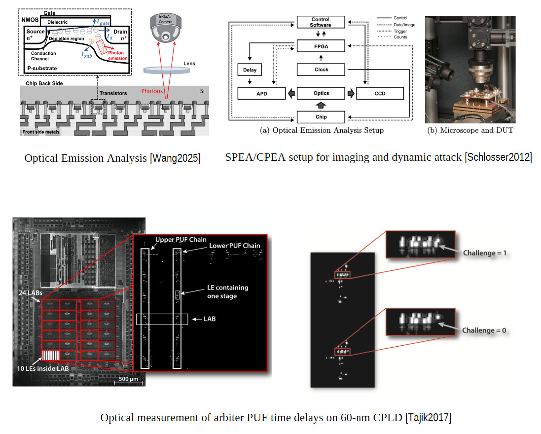
2. **Semi-invasive** attacks were coined by [Skorobogatov2005] to describe methods that require decapping and sometimes repackaging a chip to allow optical access. While this is troublesome, it is far more accessible than fully invasive attacks. In recent years, the math has gotten better: high-performance ICs are usually flip-chipped and many expose the die substrate from the package for heatsink attachment. [Amini2021] showed that for such devices one only needs to polish the backside to gain a powerful attack surface. Despite this, compact 3D-ICs, multilayer and multi-chip modules (MCM) used in phones and other compact multifunction ASICs often have the secure core obscured by other chips. [Rodriguez2019] showed that optical access can still be of value for these by triggering glitches through the chip edge with Lateral Laser Fault Injection (LLFI). Examples include passive (PEA) and active (EOFM) optical analysis, laser fault injection (LFI), spatially-resolved power analysis, and body bias injection (BBI)[Maurine2013].
3. **Invasive attacks** are typically performed by adding and removing material from the layers of an IC with a focused ion-beam (FIB) machine to observe and change metal voltage and continuity. There is very little one cannot do with such a machine, but very few who can afford them and know how to use them to their full capability. To drive an opponent to such methods is a form of economic victory, and aside from relatively low-cost multifunctional features like intrusion-detection mesh, the best response is probably to ensure nothing of value persists on the IC when powered off.
## A Selected Bestiary of Side-Channel Threats
### #1: The “inside man”: Stop pwning yourself!
A classic trope in heist films is the “inside man” and the “dupe”. Both are trusted to access secure areas, but the inside man is an of the heist crew, while the dupe unwittingly serves the crew’s ends. In hardware security terms, the “inside man” is a _hardware or firmware trojan_, a deliberately-inserted flaw that can be leveraged to bypass access controls. While catastrophic if successfully executed, compromising security hardware at manufacture requires extensive real-world subversion efforts and is mostly out-of-scope, although some dynamic reconfiguration, shuffling, and masking strategies can make it harder for a single trojan to be sited correctly or leak useful information, essentially by making it hard to place a hidden, immobile trap where it will actually be stepped on.
The “dupe” of hardware, on the other hand, is an underappreciated danger. Melvin Conway wrote that _“Organizations which design systems […] are constrained to produce designs which are copies of the communication structures of these organizations”_. This law, applied to software, came to be known as Conway’s Law. As the size and complexity of secure ICs grows, it becomes increasingly relevant to hardware too. ASICs are built with huge numbers of often-proprietary, black-box IP cores, connected by on-chip network. “Less critical” swathes of design are left in the hands of junior engineers or AI tools, while the most security-aware designers work on the secure sections. Unfortunately the modules of an ASIC are cross-cut by power rails and thermal concerns, which can allow secure modules to interact with public-facing modules in ways a canny attacker can use to infer secrets.
This may seem obscure, but many of the most impactful hardware vulnerabilities of the last decade, could be considered this sort of “dupe” attack; _Spectre_ and _Meltdown_ exploit speculative execution and caching (performance features) to leak usable information about protected memory that the MMU (security feature) protects. _Hertzbleed_ [Wang2023] attacks leverage the unintended coupling of processor activity to remotely-detectable timing information through power-efficiency mechanisms like frequency scaling and core-scheduling.
Techniques like _JitSCA_ [Schoos2023] use the unintentional voltage-sensitivity of on-board clock-generators to proxy side-channel attacks on PDNs through world-facing digital data ports like HDMI even across galvanic isolation. _Jittery JTAG_ [OFlynn2024] showed JTAG and SD card interfaces are also vulnerable, and that even externally-clocked “slave” signals passing through on-chip registers gain an angle modulation from gate threshold voltages fluctuating with supply voltage. This is treated as though it was ADC sampling and shown to leak about 5X slower than analog traces taken directly from the victim’s PDN.
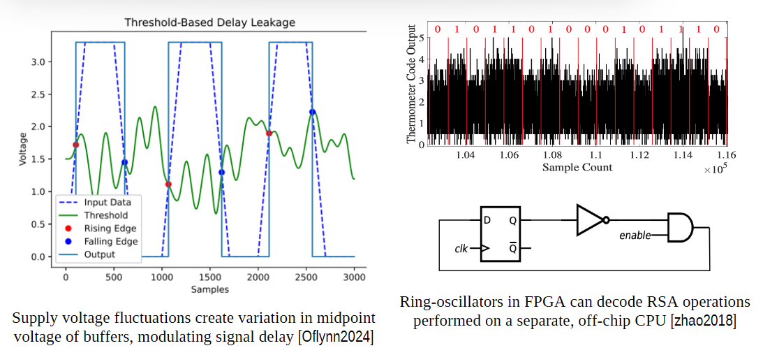
Such “inside man attacks” extend to fault injection – one can dupe a device into glitching itself. Arguably _rowhammer_ is a self-inflicted fault injection attack; corruption of memory shouldn’t happen by normal usage patterns, but lazy efficiency-minded design by DRAM manufacturers combined with clever manipulation of the trusted CPU allowed glitches to be injected into memory cells even without directly accessing them.
More traditional voltage glitching can also be done remotely. A seminal example was the ARM TrustZone attack called _CLKSCREW_[Tang2017]. It leveraged control of the processor’s Dynamic Voltage and Frequency Scaling (DVFS) registers (the dupe) to induce controlled glitches in cryptographic operations, allowing code signing keys to be determined. Following this, similar software-induced voltage fault attacks showed it was not a one-off problem: _VoltJockey_ [Qiu2019] and _Plundervolt_ [Murdock2020] showed Intel SGX was also vulnerable. ICs and devices that don’t permit control of their power supply are not immune. While FPGA-based ring-oscillator sensors and power-wasting covert channels are well-known,[Mahmoud2022] showed an attack that used gated power-wasting in an FPGA could create spikes in power draw faster than the supply could respond, sufficient to use for voltage glitching the on-chip CPU core.These sorts of attacks may seem to be less relevant to specially-constructed cryptographic hardware which traditionally has been dedicated to a single user and process, but the rise of cryptocurrency has created a market for cloud/multi-tenant hardware. Running multiple unrelated workloads on “industrial scale” platforms is much cheaper than provisioning dedicated hardware for each user, so these attacks must be considered seriously.
A malicious user might rent compute on a device, then use such types of remote attack to either extract keys to masquerade as the service provider, or extract secrets from co-tenants on the same device. The conditions needed to successfully attack are trickier to meet than traditional hardware attacks, but the cost to scale and personal risk for a remote attack are very, very low. As attributed to Stalin, _“Quantity has a quality all its own”_; a single-use attack with a 1% chance of wallet key extraction would be useless trash against any single target but would make its user filthy rich if spammed into crypto-processing data centers across the world. Threats with low probability and high impact are very difficult to quantify and deal with; luckily there’s a mental shortcut that helps protect against all forms of “inside man” attacks.
#### Defending Against Inside Man Attacks
The fundamental cause of self-inflicted information leakage like this is interdependence of behavior across security boundaries; that is, the failure of isolation. Just because one designs a system modularly and draws moats and boundaries does not actually cause the universe to decouple causality between its various parts. Inputs are not just inputs; outputs are not just outputs.
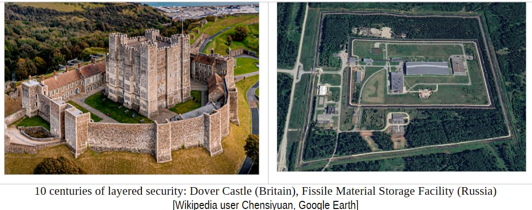
Essentially, it’s not a new class of side-channel, just a recurrence of the same old side-channels within an IC. Reduce the circle of trust from entire TEE down to just the secure enclave. If the enclave by itself is considered a secure IC and can be made resistant to side channel leakage and fault injection by itself, then “inside man” side channels residing within the larger TEE can not be usefully exploited even if they exist. **Secure the keep before the walls.** Trust grows outwards from the center.
### #2: Power Pins: classics are classic because they never stopped working
Some of the first side channel attacks on secure ICs and systems were
performed through power analysis. Any data-dependent variation in power
flow magnitude or timing conveys information, and despite heavy research
investment in _dual-rail & balanced logic_, _masking_, and other
techniques, it is still extremely difficult to guarantee the absence of
information leakage from secure processing into the power distribution
network.
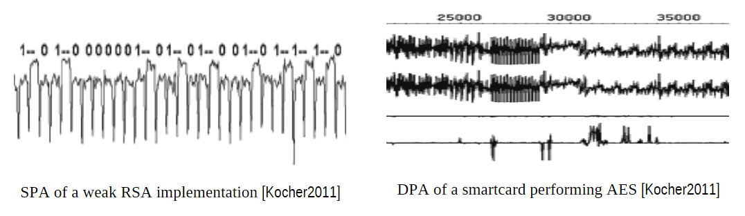
_Simple power analysis_ (SPA) just looks at time-varying current. Modern
practice at least attempts to reduce time and power variation during
cryptographic operations, and that, combined with shrinking transistor
size and ballooning gate count, quickly made SPA obsolete for secret
extraction by itself. Where it still shines is detecting the timing of
critical operations like hash verifications, EEPROM writes, and security
bit reads in order to trigger data collection and fault injection in a
world with nondeterministic cache latency, multitasking, internal clock
generation, etc.
_Differential power analysis_ (DPA) is the successor. It increases
side-channel signal-to-noise ratio by collecting many traces, assorts
them into bins based on key or intermediate value hypotheses, and
differences bin pairs. Uncorrelated effects like noise and unrelated
switching are suppressed by the averaging, while repeatable effects are
removed by the subtraction. What remains is a time-varying significance
test for each possible key byte. With an understanding of the
cryptographic algorithm and this technique, attackers can efficiently
recover keys buried in noise that would defeat SPA. There are both known
plaintext and ciphertext-only versions. Current best practice treats DPA
as part of the canonical threat model – it is cheap, effective,
well-understood, and any design vulnerable to it is not good enough for
production.
_Correlation power analysis_ (CPA) is an improvement to DPA introduced
by [Brier2004] that gets more information out of trace data by
assuming the magnitude of the differential spikes is proportional to the
number of bits changed or hamming distance. This has been shown to be an
effective assumption to use to guide search, greatly reducing false
positives suffered by DPA and accelerating key extraction. CPA is
commonly used nowadays but is ultimately limited by the same factors as
DPA. There are ways to increase statistical power using pre-profiled
_template attacks_ and _deep learning_, but these are not specific to
power analysis and indeed may attain their best performance when using
spatially and modally diverse signals streams.
There are less-common _static power analysis attacks_ that use
clock-stopping to pause encryption at a known point so slower methods
can be used to measure the leakage current of transistors or their
states' effect on impedance of the power distribution network
(_LeakyOhm_ [Monfared2023]). While more demanding to use because of
their requirement for static conditions, they require relatively cheap
hardware and have been used to break tough defenses, like dual-rail
precharge logic [Fadaeinia2024]. This latter paper is an object lesson
in how things like clock reliability are key to defending against
seemingly unrelated attack vectors like power leakage.
_Power glitching_, by undervolting or overvolting at specific times, can
stop clocks, prevent key checking, stop non-volatile memory writes, and
prevent lockout mechanisms from working. Although PDN capacitance makes
power glitching a much slower and coarser than other forms of fault
injection, its power to bypass security mechanisms empowers other
techniques in ways that cannot be ignored. Interestingly, a technique
called _fault correlation analysis (FCA)_ introduced by [Spruyt2020]
is able to analyze time and data-dependent patterns of induced faults to
as an indirect method of power-analysis, allowing attackers to use
cheaper tools or bypass some types of filtering and regulation.
#### Defending Against Power Attacks
_ **Secure Logic** _
The standard recommendation for protection against power attacks seems
to be "use masking", along with "use constant-power logic". The
former is popular because it has provable security properties and can be
implemented at the RTL level, avoiding messy details of gate
implementation or physical layout at all (and is amenable to FPGA use).
The latter because it can be smaller and simpler than masking, and it's
an endless goldmine of papers for people who like to design their own
logic families. Both of these can work, and both are expensive to
implement and can be broken.
While they can attenuate signal by up to 200x, a not-insignificant
amount, constant-power and masked logic families are not perfect and
they exact a high price: Dual rail logic's security depends on balanced
rail capacitance, something hard to guarantee in synthesized Verilog.
Dynamic logics are vulnerable to clock misalignment and glitching, can
be defeated by static analysis and optical trickery, and are not
well-supported by standard logic libraries. All require at least 1.5-2x
the area and power of standard CMOS (some up to 8+x). Gate-level masking
has similar limitations (35 families of constant-power logic and 5
families of masked logic are compared in [Sanchez2022]). The families
with the best figures of merit do not come in standard libraries --
they require custom circuit design and layout and are poorly
characterized, requiring the designer to allocate extra time and
resources to ensure any designs made with them are reliable and secure.
This cost may be acceptable for a large company using only in-house or
open-source secure IP implemented a single IC process as it can be
amortized across multiple designs, but is unsuitable for the SILO
plug-and-play technique “toolbox”.
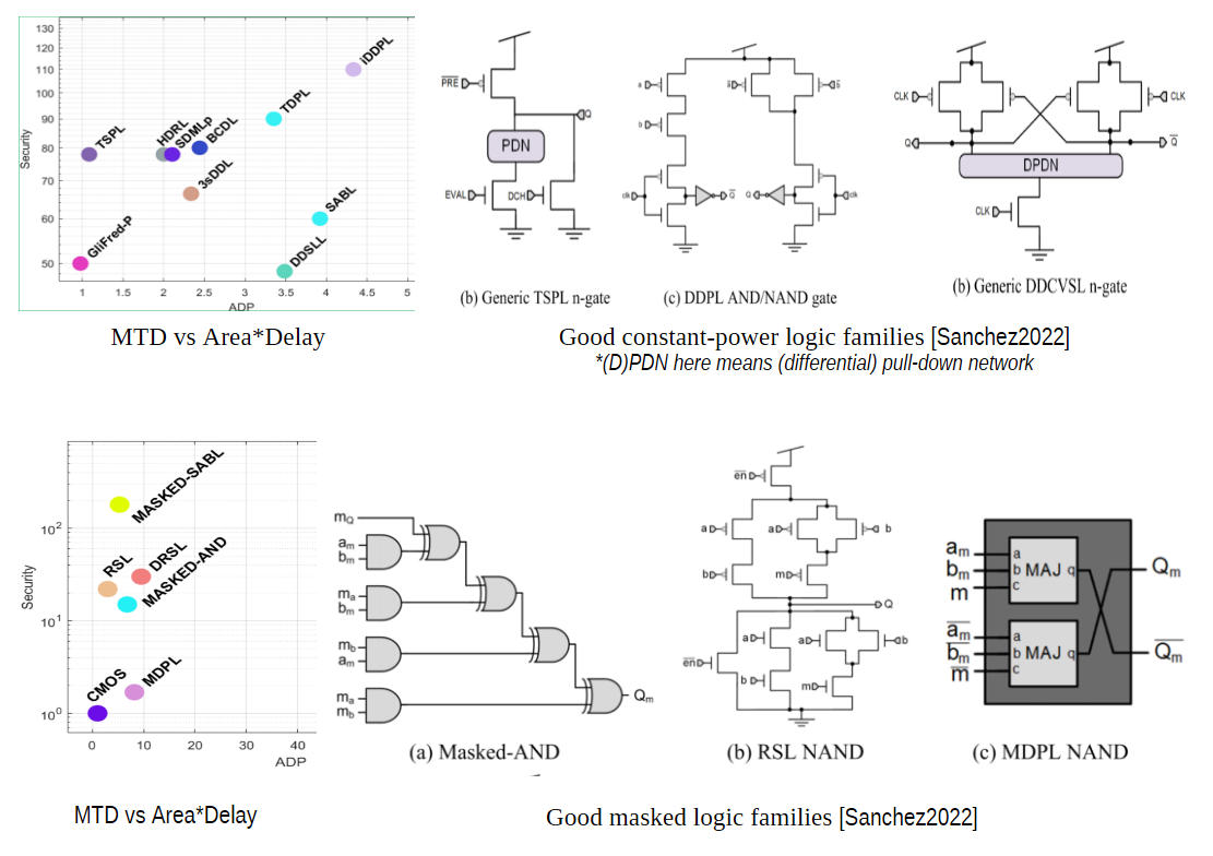
RTL-level _masking_ and _Threshold Implementation_ are very well studied
and can work quite well, but come at a similar cost to constant-power
logic: a very similar increase in area, delay, and power. Their
security, although mathematically provable under certain approximations,
is not ironclad. PDN crosstalk between masking shares has been shown to
lead to usable correlation in shares for side-channel attacks.
Additionally, a 20x increase in area is not unheard-of with threshold
implementations and higher-order masking, which is a very heavy price
indeed. This is the sort of technique that appeals to mathematicians and
computer scientists conceptually but the experienced IC engineer applies
only when every other trick has fallen short of the needed security.
Even then, those skilled in the art would be well advised to white-box
model and root-cause analyze to sniff out where leakage is coming from
before reaching for the big math hammer and smashing leaky computation
into less-comprehensible shards.
That all said, those forced to secure algorithms in FPGAs may have
little choice in the matter. Without access to precise place-and-route,
alternate logics, or analog design, they must use the tools that remain.
One can hope that someday FPGA makers will provide some of these tools
as primitives for secure enclave construction in special FPGA & CPLD
families.
_ **PDN Filters** _
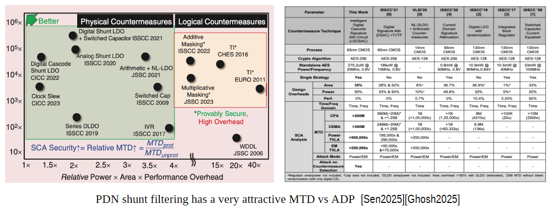
When searching for papers related to power filtering & regulator design
for side channel defense, two groups come up the most: Intel Research,
and SPARClab at Purdue. The results are quite promising compared to
logic-focused techniques like masking and secure logic. Rather than
trying to prevent side-channel leakage in the secure computation itself,
power filtering treats it as a quarantined black box, blocking PDN
leakage with a special power filter circuit.
Broadly, such circuits are either switched-capacitor or digital linear
filters with randomization applied to them such that patterns in power
consumption are both attenuated and obscured. This is, in principle, the
same outcome that constant-power logic and masking seek, but outsourced
to specialized hardware.
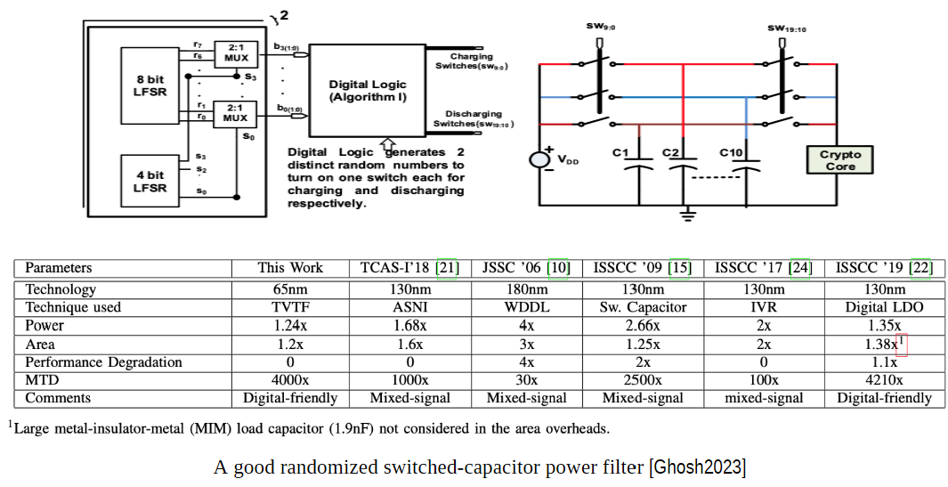
Switched capacitor filters use mosfets and capacitors to store and
transfer power "packets" from the supply to the filtered load. Some
are regulators, which maintain constant load voltage; others (like TVTF
[Ghosh2023]) function as time-varying nonlinear impedances. Early
efforts tried to just use the flying capacitor to temporally quantize
power consumption, but this was quickly found to not yield enough added
security to be worth the trouble. Modern work splits flying capacitance
into multiple phases (very low overhead in CMOS), and randomizes their
switching order and timing to perform "stream transposition
encipherment" of power consumption in both time and frequency.
This seems to work well; published works show a typical AES or RSA core
gains up to 1500x improvement in MTD for ~100 pF of flying capacitance
and ~20% added power. In return for this investment, a well-designed
switched-capacitor filter can completely isolate its secure enclave from
overvoltage, undervoltage, impedance probing, and blackout. A well
designed circuit with large-enough capacitance stores enough energy to
function as a "secure UPS", allowing one to securely erase secrets and
possibly write a nonvolatile alarm flag even with external power
completely removed. For some applications this feature may be worth the
area cost.
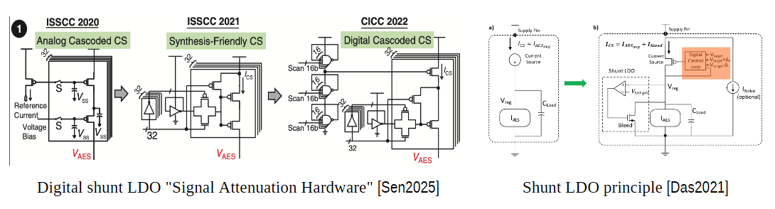
Best among linear filters are the "_Current Domain Signature
Attenuation (CDSA)_" family of filter-regulators developed by SPARClab
since 2016; they implement a slow envelope-tracking constant-current
source implemented as a randomized digital "LDO" coupled to a shunt
regulator to regulate the output voltage without allowing any useful
variation in load current to be measured.
This technique necessarily wastes power (typical efficiency 50%) but
provides tremendous MTD improvement with less added area than
constant-power logic families trying to implement the same idea at the
logic level. Linear filters and regulators need less space and provide
somewhat better security than reported switched capacitor circuits, but
cost more power as they must dissipate the maximum of possible power
consumed to hide patterns rather than "transpose" or "time-shift"
them. Work on this type of device has progressed from basic analog
implementation, to digital-synthesis-friendly, to the current
state-of-the art in [Ghosh2025] with an added sense circuit to detect
brownout attacks that would cause the current-source filter to leak
information.
Our recommendations against power attacks:
- **Filter power for sensitive islands**. Power is data; do not mix red and black.
- **Secure PDN filters beat secure logic** : The same or better MTD for
less added size.
- **Combine power filtering with other techniques** like masking,
scrambling/shuffling, and careful layout for multiplicative
improvement.
- **Adding noise works** , but only when you already have good power
filtering.
- **Isolate power for mask shares.** Crosstalk between mask shares
through PDN creates exploitable correlation. [Seckiner2022]
### #3: Electromagnetic Waves: TEMPEST on a chip
EM attacks are non-invasive and potentially long-range. The first use of
EM emanation monitoring to break cryptography is probably the
now-declassified 1943 discovery by Bell Systems that the 131-B2 mixer
used in the one-time pad SIGTOT system emitted enough EM to extract
plaintext remotely from 80+ feet away, and later, a quarter mile on the
signal line [Friedman1972]. A seminal paper by Van Eck in 1985 showed
that such attacks could be cheap and capture video from CRTs. The
security impact of EM emanation monitoring has apparently fluctuated
over the years; it is harder to correlate EM emission with chip
operation than power variation, and hardware to capture broadband EM
signals was not as accessible as digital oscilloscopes until fairly
recently.
This _far-field analysis_ is the most familiar and recognizable form of
EM attack. A shadowy figure in a van packed with antennas and blinking
lights is classic Cold War cinema technomagic. Technology always devours
its own aesthetic, of course, and nowadays that van's equipment fits in
a small briefcase or handheld USB _software-defined radio_ (SDR) device.
Despite the ubiquity of strong encryption, thanks to the availability of
commodity SDR, high IC clock rates (leading to greater emission), and
the presence of wireless connectivity in almost every electronic product
have conspired to create a target-rich environment for EM attacks.
Notably, researchers have demonstrated far-field EM side-channel attacks
at distances of several meters; [Camurati2018] extracted an AES key
from an IoT device running mbedTLS at a distance of 10 meters using a
sensitive radio setup. The security firm Fox-IT [Ramsay2017] showed
that cheap SDR hardware could steal an AES-256 key in minutes from ~1 m
away through detected EM side-channel emissions. It's notable that when
radio hardware is integrated into an IC, it often can become an "inside
man", leaking PDN fluctuation through unintended modulation of
oscillator phase noise or power amplifier harmonics. This is a failure
mode at least 70 years old, where early encrypted radios transmitted a
subtle plaintext "ghost" signal that undermined the entire point of
encryption.
_Near-field analysis_ is a class of attacks created in response to the
massive integration complexity of modern ICs. Very small magnetic or
electric field probes are positioned in specific locations and
orientations against a target chip's package. Signals captured during
operation are broadly similar to those of power analysis but far more
spatially and temporally detailed; attackers can localize specific
signals of interest separately from other activity.
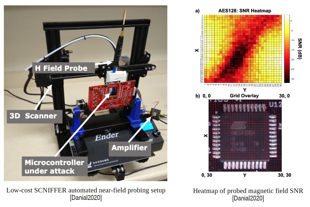
For example, in [Danial2020] a team built a low-cost EM scanning
platform called _SCNIFFER_ using a modified 3D-printer and an H-field
probe for under $500 able to automatically find the points of highest
leakage SNR on a chip and apply a key-recovery attack similar to CPA
(CEMA) against it, requiring orders of magnitude fewer traces and labor
than conventional power analysis would. This DIY scanner achieved
similar results to a professional ~$50k EM probe station.
_Electromagnetic Fault Injection_ (EMFI) also exists. Rather than
touching the power pins, an attacker can use a coil or probe to emit a
high-frequency electromagnetic pulse at the chip to induce voltages or
currents and upset transistor operation for a brief moment. EMFI is
noninvasive, contactless, and allows for spatially-resolved attack on
targeted functional units. It has been demonstrated that EM pulses can
corrupt critical operations, such as skipping instructions in a ROM or
altering a bit in a comparison. For example [Gaine2020] were able to
demonstrate the theoretical practicality of EMFI to bypass password
checking in a mobile phone processor. [Cui2017] presented the BADFET
platform and used it multiple times to root a Cisco VoIP phone: first to
enable the uBoot terminal, then again to glitch the TrustZone TEE to
execute arbitrary code. Others have shown successfully injecting faults
into SoC MMU and CPU caches, allowing instructions to be skipped and
exploit code to be injected into privileged memory spaces.
The cost of EMFI equipment has also come down: hackers have created
$100--$1000 DIY setups (e.g. using a modified camera flash or a coil
driven by a high-current MOSFET). There are open-source EMFI setups like
the BADFET, ChipSHOUTER (~$3K), and PicoEMI (~$50) now that open
this avenue for hobbyists and tinkerers.
#### Defending Against EM Attacks
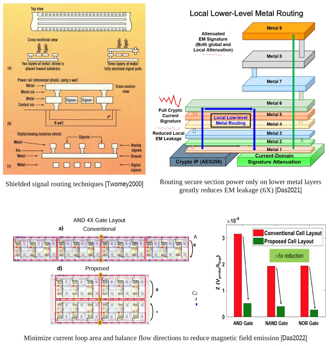
Although more complex than power analysis, EM analysis is harder to
stop. EM emission is generated by all switching processes in a chip and
spans many decades of frequency. A poorly designed shielding mesh can
even resonate with some frequencies, increasing their emission. Near
field EM is like the "big brother" of power side channel leakage,
often emitted by it, but carrying a lot more potential information in
its spatial distribution.
Countermeasures used to reduce PDN leakage like _ **voltage filtering** _ and
_ **constant power regulators** _ also help with EM somewhat by confining power
fluctuations to the secure enclave and reducing their amplitude, but the
distributed nature of EM emission means that distributed measures like
_ **physical shielding** _ are also needed. Unfortunately magnetic fields are
rather hard to stop with on-chip shielding, and metal meshes designed in
most processes only cover the front side anyway. The solutions used in
the literature tend to be to exploit the "blurry" spatial resolution
of the comparatively large pickup probes by using _ **careful layout** _ to cancel out
voltage, current, and operation at a small-enough scale that there's
nothing intelligible left for a large probe. Some designs also use _**noise
injection**_ techniques like spread-spectrum clocks, or shuffling
techniques like randomizing the execution order of operations, to
“smear” the EM signature in frequency domain.
Defense against EM fault injection is similar to voltage glitch defense
-- _ **detector circuits** _ and can sometimes detect the electromagnetic
disturbance (e.g. by noticing a glitch-induced circuit misbehavior), but
often EMFI can be very localized and fast. Shielding the device or
encapsulating it in metal can reduce susceptibility (at the cost of
weight and thermal dissipation issues). Some sensitive modules use
_ **active shields** _: metal layers on the chip carrying signals that would get
disturbed if an EM pulse penetrates, allowing detection. Plausibly one
could repurpose certain designs of tamper-proof mesh or optical fault
injection sensors to also detect EMFI.
Our recommendations against EM attack:
- **Focus on near-field attack**.
If a sensor right next to your chip can't find anything, an antenna 10
meters away won't either.
- **Treat power as a signal** : minimize loop area, maximize local
current flow cancellation.
- **Only use lower metal layers** for signals and power within the
secure enclave.
- **Don't trust constant-power logic** ; [immler2018] used EM
analysis to break dual-rail.
- **Good layout hygiene!** If just routing power nets carefully
nets a 5-10x leakage reduction, start with that before diving into
complex, high cost security methods.
- Chip layout can't protect you completely. **Shield and tamper-proof
the package.**
### #4: Semi-invasive attacks: The danger of an exposed backside
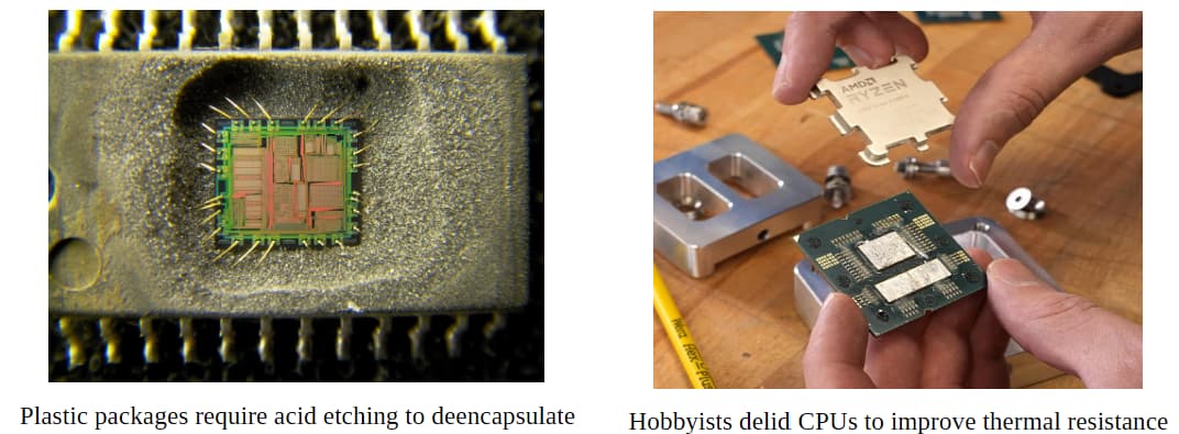
Back in the old day, ICs would be made with \<4 metal layers, visibly
large transistors, and insufficient paranoia. One could image a chip
with a visible-light microscope to reverse engineer it. Those days are
long gone; the march of progress has made transistors too small to image
with visible light, there are often \>9 layers of metal, and power is
distributed through dense meshes that obscure the transistor layer from
the front side.
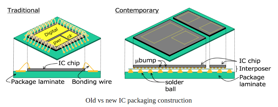
Another change is that old IC packaging had the chip soldered or epoxied
onto a grounded metal plate face-up with pads wirebonded to the package
pins. This worked well enough and is still used for lower-performance
products, but it was discovered that one could have more speed, better
heat removal, and less size by packaging ICs face-down with pads as
close to the underlying circuit board as possible. As a side-effect of
this change, modern high-performance IC packaging makes the vulnerable
backside much more available for attackers to access. The desire for
better heat removal often makes chemical decapping completely
unnecessary.
#### Electrical
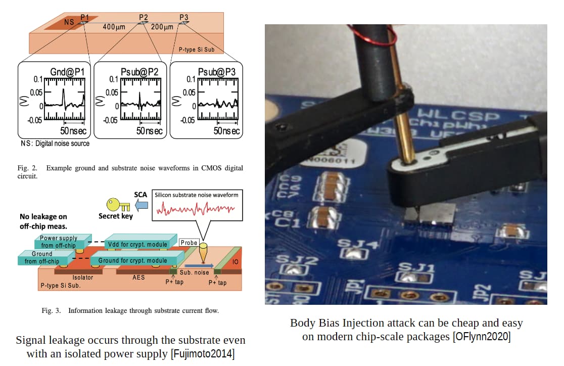
In almost all digital ICs, the substrate is relatively
conductive (1-25 ohm-cm), ubiquitously contacted to the ground net
(millions of contacts, 1-10 ohms/contact), and mostly assumed to be a
ground plane. For back-of-envelope calculation this is a fair
assumption, but so are spherical cows in physics. Side channel attacks
specialize in leveraging signals in the microvolt range, and from this
perspective the substrate serves as a way to access ground plane
voltages with far more spatial and temporal resolution than can be
obtained from PCB traces. This can be used for _substrate-probing power
analysis_ and _body bias injection_(BBI) attacks. In [Fujimoto2014]
this leakage was used to mount successful CPA attacks on an AES core in
65 nm technology from both front and back sides; one can imagine how
much more effective this technique would be combined with an automated
probe platform like SCNIFFER, while [Maurine2012] used body biasing to
change threshold voltages for targeted fault injection.
#### Optical
Silicon is transparent to NIR light (wavelengths \>
1100nm). This means that if one can access the "backside" of the
chip—the substrate—they effectively have a window into the MOSFET
layer, where all computation and data storage happens. Thanks to subtle
voltage- and current-dependent optical phenomena, attackers can perform
_optical activity monitoring_. Conversely, silicon absorbs shorter
wavelength photons and generates photoelectrons that collect in nearby
transistors, producing up to 0.7 volts “from thin air”. This is how
digital cameras detect light, and can used to perform very effective
_optical fault injection_ attacks when carefully aimed and timed.
_Photonic Emission Analysis_is a technique used in the semiconductor
industry that has been used to attack secure ICs. As transistor feature
sizes shrink, the electric fields within the channel increase, bringing
with them hot-carrier luminescence. When a short-channel transistor
switches, hot electron flow can cause a small amount of near-infrared
(NIR) photon emission. A relatively inexpensive system to detect this
emission was described in [Schlosser2012], who called it _Simple
Photonic Emission Analysis_ (SPEA). Differential (DPEA)[Kramer2013]
and correlative (CPEA)[Wang2016, Wang2025] variants were quickly
developed by analogy with DPA & CPA. Although somewhat obscure, the
attack is relatively easy to perform on chips with exposed substrates
and allows activity monitoring with very precise temporal and spatial
resolution. This threatens the security of certain types of digital
PUFs; [Tajik2017] broke delay-line arbiter PUFs using photonic
emission analysis followed by model-fitting to clone it in software.
_Electro-Optical Frequency Mapping_(EOFM)[Liu2022] uses focused laser
light to monitor voltage-induced reflectance modulation of depletion
regions in MOSFET drain and channel. Although the percent change is
small (~2 ppm), it can reliably measure logic levels in an operating
device and has potential to achieve almost FIB-like probing power with a
relatively cheap microscope attachment. PEA and EOFM are complementary
because the former detects _current_ (switching events), while the
latter detects _voltage_ (state). It's not difficult to imagine a
camera-photodetector-laser-microscope built like the RayV Lite combining
these two techniques with laser fault injection and an SNR-optimizing
automation platform like SCNIFFER.
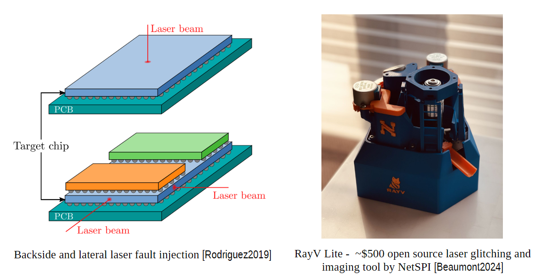
_Laser Fault Injection_(LFI) uses the same photoelectric effect that
powers solar panels and digital cameras. Shining a laser into the
silicon part of a chip causes carriers to be generated; where diode
junctions exist, these carriers accumulate to produce voltage. As every
transistor is composed of diode junctions, this process can be leveraged
to inject faults at arbitrary places and times. Some academic attacks
have used infrared lasers to target specific transistors (with
micrometer precision) to flip bits in cryptographic calculations or
disable security lock bits. This form of fault injection is already a
mainstay of “professional” labs, has been significantly refined
[Viera2020] and tooling can be built for under $1000. Laser fault
injection is most effective from the back, but can work from the front
and even the side: [Rodriguez2019] demonstrated successful targeted
glitching on the middle chip in a 3d stack with an attack they called
_Lateral Laser Fault Injection_(LLFI)
_Optical Beam Induced Resistance Change_ _(OBIRCH)_ or _Thermal Laser
Stimulation (TLS)_ is a technique usually used for semiconductor fault
analysis (like finding short circuits) which has found application in
key extraction attacks. It uses 1310 nm laser light to heat target
transistors, changing resistance and off-state leakage. This was used in
[Lohrke2018] to deduce gate voltages and extract the security key from
the battery-backed SRAM of an SCA-hardened Xilinx FPGA in “less than 15
minutes”. [Grandamme2024] showed that this thermal leakage effect was
also able to release the trapped charge in flash memory, making it
possible to modify nonvolatile security settings and bootloader firmware
of unpowered devices.
#### Defending Against Backside Attacks
Fundamental to all backside attacks is the substrate. Whether optical or
electrical, anything that goes through the backside is going to perturb
the substrate, and that can be detected and attenuated by properly
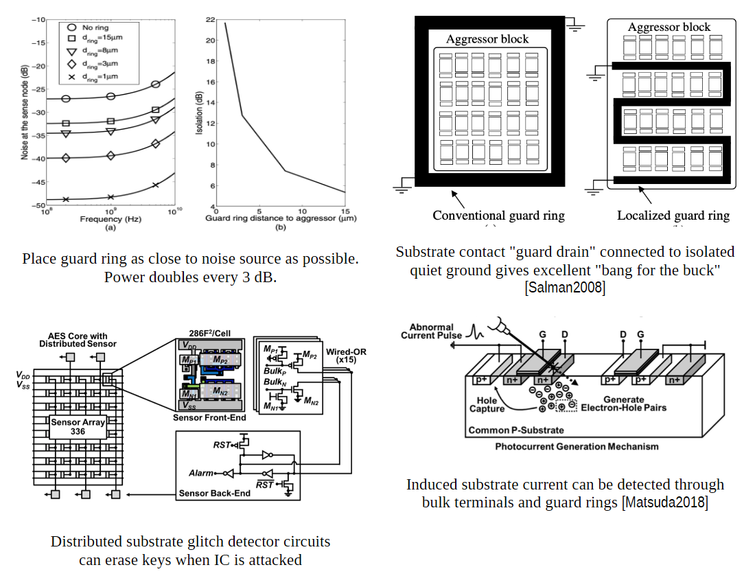
attending to the substrate. _Guard rings/bands_ are a common technique
used in mixed-signal design to protect sensitive preamplifiers and
oscillators from noise generated by "loud" digital switching and power
output stages. Adding contacts to the substrate allows draining both
internally and externally-generated noise away from sensitive nodes.
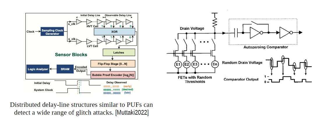
Various types glitch detection circuits have been proposed as well:
N-wells used in PMOS transistors and guard rings can collect and detect
photocurrents [Matsuda2018]; delay-line circuits like FTC
[Muttaki2022] and HEED [Nabhan2026] are affected by a wide range of
fault-injection attacks in ways that make them usable as security
watchdogs.
That said, the range of backside attacks is wide and their power is
great. To expect any design to resist all possible attacks without even
a single metal layer is surely asking too much -- **why not just cover
the exposed backside?**
One simple strategy is to use integrated impedance sensing to monitor
the integrity of a backside shield, plane, mesh, or package such that
any hole large enough for meaningful backside access will be detected
and trigger key erasure. [Tahoura2024] showed that even the on-chip
PDN itself can be impedance-profiled to detect the modification of the
adjacent PCB or removal of heatsink. While this idea seems like it would
need careful testing to be made reliable, it's simple, cheap, and will
likely frustrate both power analysis and fault injection as a side
benefit.
Alternately, one can simply integrate the secure IC into a stack or
sandwich such that its substrate is covered by another IC. If done
properly, to gain access to the backside is to disassemble the stack and
lose any secure information. Two of the same IC could be attached
back-to-back, or a multi-chip module could be constructed with a
non-security chip providing the needed backside protection. One could
presumably use the capacitance or EM parameters of the second chip as a
random physical property for an anti-tamper PUF as well.
Moving up-market, some processes have _backside buried metal (BBM)_ or
_backside power delivery networks (BS-PDN)_ as process options. These
thin the substrate, layer it with one or more metal layers and connect
them to the front side with _through-silicon vias (TSVs)_. While
invented for better ground contact and power distribution, backside
metal offers a ready-made path to integrated backside shielding if
process and cost permit. While [Miki2019] found that applying metal to
the backside alone provides a meager 3dB improvement in EM attenuation,
it is likely that grounding such a shield with TSVs would improve
matters, and even leaving it floating would still greatly enhance the
protection afforded by other substrate noise and EM hygiene techniques
by blurring localized signals with their protections.
[Gao2023] describe the dual-use of a shield laid out as a random
Hamiltonian path and stimulated with a pseudorandom sequence for both
shielding and EM signal masking. This was apparently quite effective,
and one can imagine that segmenting such a shield and putting it in a
package with heterogeneous material fill similar to the structure
suggested by [Tuyls2006] would allow it to also serve as a
tamper-evident PUF.
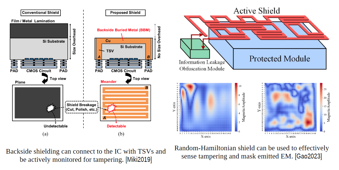
_ **Our recommendations against backside attacks:** _
- **Cover it!** Secure & shielded packaging is an entirely different layer than layout, circuit,
logic, and algorithm. It's also relatively cheap & easy for the
benefits.
- **Don't trust, verify.** A fence is only secure if watched. Active
shielding costs little extra power or area, and helps against both
passive and active attacks. Even cheap secure packaging can be made
much safer by active scanning and noise stimulation.
- **Differential logic is not safe.** If researchers can optically
flip SRAM bits, they can resolve dual rail logic channels.
**Especially in FPGAs.**
- **Noisy shields rule!** While generally not sufficient on its own, a
bit of pseudorandom signal pushed onto shield nets can vastly
improve system MTD when combined with careful placement & routing of
secure circuits.
## Selecting defenses: Getting to "good enough"
The world of secure hardware has more attacks and defenses than any single paper or review can cover. We have covered threat scenarios that are easy, common, ruinous in undefended, and amenable to automation. The long tail left uncovered tend to be situational, experimental, exotic, expensive, or impractical -- acoustic, thermal, radiation/particle-beam, FIB, etc.
It is always possible that someone out there will build a homemade proton-beam apparatus in their basement and use it to inject charge through defensive mesh, or have access to a SQUID micro-magnetometer array for extracting fields below the noise floor. Perhaps specialized MRI microscopy can extract chip imagery and memory bits, or stereotactic X-ray machinery can focus many beams to intersect at precise locations through shielded packaging. Perhaps interferometric microphony can detect ultrasonic vibrations caused by the heat fluctuation or magnetoconstriction of individual metal lines buried deep inside in a chip. Perhaps polarization-sensing quasi-optical terahertz holography will grant unprecedented monitoring of the shifting resonances of PDN branches and mosfet channel state. Perhaps there will be chips whose security is broken by techniques like this; perhaps it has already happened.
But most likely, someone left the JTAG bus unsecured and it can be used as a probe to infer PDN voltage or abused to inject glitches. Or the Bluetooth frequency synthesizer is modulated ever so slightly by digital core noise. Or their AES core has mask traces on the same power line, creating an exploitable correlation. Or they didn’t shield and route their differential logic signals and an EM probe in just the right place picked up the difference signal.
Far more is stolen by crime of opportunity than by high-effort heist. Unlocked doors and open windows are greater dangers by far than safecrackers and tunnels. The cruel arithmetic of OPSEC teaches that human psychology tends to fixate on good stories: the rare and dramatic. They are not what gets spies caught and fortresses taken. Good security is much more like hygiene – multiple layers of well-tested, consistent procedures performed without fanfare or heroics. Communication channels filled with data regardless of the volume of actual traffic, guard rotations which vary independently from ongoing work, sentry procedures that check ID the same regardless of visitor rank or importance. Consistency is virtue and boring is success. Security wins when nothing happens.
In light of this, our recommendation to secure IC designers of the present and future is to develop and rigorously characterize a standard set of the following mostly-orthogonal techniques in their processes of interest. Many of them are able to be wrapped around arbitrary “black box” objects and can thus be easily reused and recombined to find the best security vs performance tradeoff. Perhaps someday this will yield open source secure standard cell and analog IP core libraries for modern processes.
A _**side-channel isolated logic oasis (SILO)**_ is the cheeky acronym given to this concept. Ancient Romans had a standard marching camp called the _castrum_. These were constructed by legionnaires _every night_ in _2-3 hours_ (after marching all day!) following a plan that hardly changed over a thousand years. Balancing security and ease of construction, the standardization of these camps conferred to Roman forces a significant military advantage in hostile territory. The simplicity was what made them practical. A SILO is our vision of a chip-designer’s _castrum_, a good-enough set of easily deployed, standardized security techniques that let us sleep at night without fear of Gauls.
From the techniques discussed previously, we suggest a layout like this in general:
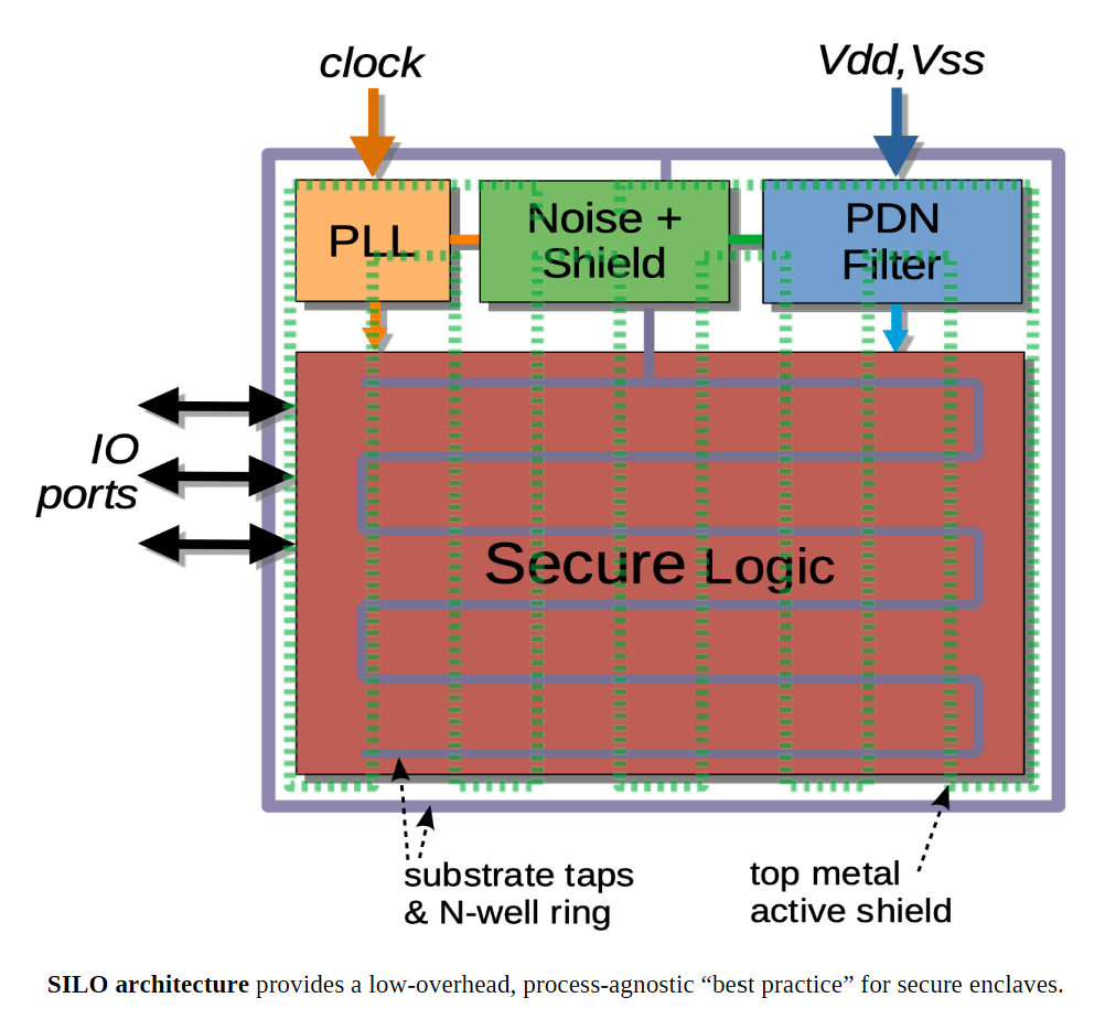
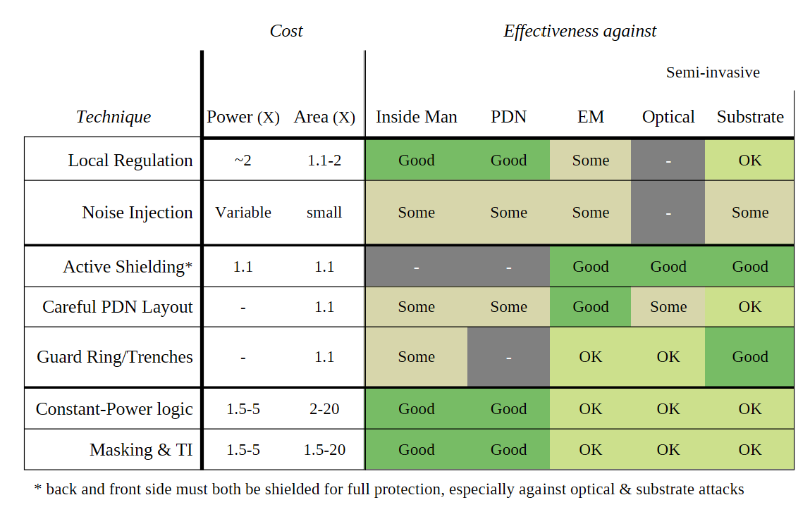
The following specific techniques have the best figures of merit among papers researched for this report and comprise “low-hanging fruit” for any secure enclave design.
- PDN filter or regulator, with noise injection if needed [Ghosh2025][Das2021]
- E&M-aware low-metal PDN wiring within oasis [Das2021][Das2022]
- distributed substrate taps on quiet or noise-masked rail [Salman2008]
- noise-stimulated "active shielding" security mesh above [Gao2023]
- internal clock-retiming PLL or at least clock glitch detection
For higher security, one can add (for increasing cost):
- tamper-evident packaging (PUF or active shield-integrated)
- N-well, bulk terminal, or ring-oscillator-based fault-injection detectors [Muttaki2022]
- arithmetic masking techniques or special logic [Sanchez2022]
- scrambling and/or threat-adaptive defense posture
Based on papers read for this work, even the baseline techniques presented can yield MTDs \> 1B for all most common attack modalities, before even considering heavier algorithm-level methods like mask shares and threshold implementation. What is described is a combination of "common sense" best-practices for IC low-noise and EMC design, juiced with tripwires and entropy to foil intentional attack. We have, in a sense, defined the walls and roofs of the secure enclosure, while leaving the contents to be design-specific. The entirety of the "baseline" hardened SILO should be implementable with between 50 and 100% extra area over an unprotected naive logic IP block, and can be wrapped around such blocks without requiring heavy modification.
## The Coming Storm: Democratization of Automated Attack
Looking five years ahead, a few trends stand out as potentially transformative to the security landscape and will likely force reassessment of what “appropriate” secure design looks like for trusted compute and secure enclave hardware.
### Open source & commodity tools
As more open-source hardware projects for security testing emerge, the community of potential attackers grows and the barrier to entry lowers.
EM attacks are enabled by software-defined radio (SDR) hardware, which has become much cheaper since Broadcom released the BCM21551 single-chip 3G SDR IC in 2007. Open-source platforms like GNU Radio have transformed data acquisition and processing from a specialized RF engineering task into code, with the common platform making reuse of others' work easy. Now a full range of options exists, from $10 receive-only RTL-SDR USB dongles to $5000+ multi-channel USRP boards with gigabit Ethernet and onboard FPGA processing.
Power analysis, voltage and clock fault injection are similarly enabled by platforms like ChipWhisperer, which brings a mature ecosystem of standardized code and methods to power analysis and voltage fault injection. Seemingly the de-facto standard for power attack papers, it is sold in performance tiers costing from $50 to $5000. Newer iterations like ChipWhisperer-Husky seem to be inspired by the USRP, providing features like FPGA-based onboard trace analysis for a similar price point.
Optical attacks are more esoteric, but NetSPI's development of the incredibly clever RayV Lite seems to be ongoing, and it manages to remove the need for a microscope by integrating an objective lens directly into a 3D-printed precision motion stage adapted from the OpenFlexure, yielding laser glitching and self-mixing interferometry-based optical analysis capabilities for around $500
[Beaumont2024]. Yes, you have to build it yourself for now, but that's not likely to be the case for long.
Another nascent development is _multi-modal side-channel analysis_. A side-effect of the availability and standardization of these tools is that it becomes practical to combine them. By capturing and analyzing multiple side-channel signals simultaneously, it is possible to raise the SNR of leakage that would have been undetectable when defenses were designed. This is analogous to the military doctrine of combined arms; sometimes a combination of methods is more effective than the sum of its parts.
An attacker might use a machine learning model to fuse SDR-gathered EM
probe data with PDN traces, or use multiple probes as a sort of phased
array or polarization-sensor to strip out noise more effectively.
Passive analysis might allow adaptive tuning and correction of active
attacks, perhaps in multiple stages analogous to software privilege
escalation exploits. An attacker might decide that a static attack like
leakage or impedance analysis will extract the information they desire,
but the target has an internal PLL to prevent clock glitching. To
overcome this, they could use a power brownout glitch, except the target
also has a brownout detection watchdog.
So the attacker puts a set of instruments together: First a
ChipWhisperer generates a controlled brownout just above the level that
trips the alarm. An SDR whose FPGA is programmed to detect and count PLL
clocks sends a trigger signal to an EM pulse tool positioned over the
PLL, momentarily spiking its voltage below the threshold of operation to
freeze it at a precise clock count from the detected start of an
encryption or memory access operation. With this process automated and
repeatable, stepping through encryption steps and extracting bit counts
or hamming distances from measured leakage is almost trivial.
Such an attack would be quite the masterpiece of reverse-engineer's art
in the past, a dissertation-worthy labor to find and fully develop to
practicality against a single target. With commodity hardware and
interoperable open source platforms with standardized APIs and plugins,
an ambitious and smart undergraduate student could perhaps be guided to
develop it against a well-understood target in a couple of weeks. Such
is the progress this era's security engineers must contend with, and
it's just beginning.
### Machine Learning and AI
One might point out that "guided" and
"well-understood target" are doing a lot to hedge the preceding claim.
This is true, so it's finally time to invoke the specter haunting computer science: AI.
In this work, distinction will be made between _machine learning (ML)_
and AI. ML is the pre-LLM name commonly given to "low level",
mechanistic model-fitting and statistical techniques like clustering,
classifiers, dimensionality reduction, etc and this distinction matters for
signal processing. An
ML-augmented attack typically involves something like statistical
profiling, template generation, event-detecting matched filter or
neural-network training, probe SNR-maximizing search algorithm, and the like.
These types of methods are less sexy than telling Jarvis to hack the Gibson
for you, but they're small, simple to implement, and
can run inference or classification online with data collection at full
data rate. Building blocks to develop higher-level methods, and
absolutely essential for analysis-triggered active attacks.
Deep learning models (CNNs, autoencoders, etc.) have been demonstrated
to learn features from raw traces, often achieving higher success rates,
especially powerful in “profiled” scenarios (where the attacker can
train on a device similar to the target). _Deep Learning Side-Channel
Analysis (DLSCA)_ allows trading off increased compute power against the
time and effort required to gather more traces. Profiling needn't be on
a per-target basis, either. A cross-device deep learning attack
framework called _X-DeepSCA_ was shown to generalize across different
chips, reducing the number of traces needed and making attacks more
portable. The result is a faster time-to-key recovery and less need for
target profiling. _Differential Deep Learning Analysis (DDLA)_ has shown
the ability to recover keys from protected implementations, including
those with masking, without explicit leakage modeling.
Traditional higher-order attacks require combining leakage from multiple
points in time (e.g., via a product combining function), which amplifies
noise. Deep learning models can implicitly learn these non-linear
combinations during the training process, effectively performing
"automatic" higher-order attacks. This reduces the expertise required
to attack masked implementations; the attacker no longer needs to
mathematically derive the optimal combining function. While no
standardized platform exists yet to store and deploy these models, the
existence of "open weight" LLM models and the general awareness shift
of the value of model weights as first-class entities alongside code
makes it likely that this will change.
LLM-based tools unlikely to be usable directly for performing attacks,
but agentive frameworks make it easy to empower them with the
lower-level tools they need to do so. Given the rate of AI adoption in
the software security world, it seems a safe bet that in the next few
years there will be commercialized “hardware attack copilot” LLMs
trained on IC documentation and vulnerability databases, capable of
interfacing with and controlling common attack hardware and test
equipment. With a part number, image of board or chip die, JTAG scan
chain data, or even EM traces, such an AI could determine what was being
attacked, find forums and guidance from others, suggest effective attack
strategies, locations, timing parameters, templates, even generate
needed software-side code or configuration for hardware. ML-based agent
plugins can perform automated tuning and execute on programmable
components like FPGAs present in hardware that supports it. While this
ecosystem doesn't exist yet, it seems unwise to bet on it remaining so.
### Cyberpunk is Just a Western with Neon and Chrome
> Shenzhen, 2035:
>
> In a nondescript light industrial park, there is a nondescript e-waste
> repair and recycling firm where the lights stay on late into the night.
> If you were to visit and somehow be let in, you would initially see
> nothing unexpected. Rows of workers bent over microscopes, hot air
> solder stations, IR hotplates, BGA reballing setups, rolling carts and
> baskets of shucked electronic device husks and extracted components;
> just another colony of unglamorous but necessary decomposers dwelling in
> the root system of global high-tech consumerism.
>
> But if you knew about a particular nondescript door and opened it, you
> would find another room, also with rows of workers under harsh white
> lamps disassembling phones, laptops, and small plastic devices -- but
> they are not what matters here. The true heart of this operation betrays
> itself with frenetic blinking of LEDs and roar of enterprise server
> fans: A rack of compute blades and bundles of network cables leading to
> shelves stacked with test equipment and what look like 3D printers.
>
> Seen up close, each has an electronic device or circuit board secured
> to its bed, wires splaying off to the humming test equipment.
> Occasionally their heads twitch, seemingly without effect, while
> indicator lights flash and text scrolls by on attached displays. Every
> once in a while one of the machines emits a "ding" noise, retracts its
> head, and lights a large green lamp; a worker shuffles over with a cart,
> removes the circuit board from its bed and replaces it with another.
> This is their job. Every day hundreds of phones, laptops, 2FA dongles,
> and hardware crypto wallets are plucked from the detritus of the first
> room and passed into their hands, then to the machines that sent the
> company owner's children to Stanford. They’re majoring in engineering
> and business.
>
> This nondescript company is one of dozens of cybercrime-affiliated
> electronic chop-shops in Shenzhen, and aside from recovering valuable
> chips for resale from old phones and replacing broken screens, it
> operates a hardware cracking assembly line with its in-house labor pool
> and a bank of AI-assisted automated side-channel attack machines. Its
> technical management frequent dark-web forums to buy, and sell attack
> profiles and share techniques to use with their jailbroken local AI and
> modded open source hardware. If it's raided, another equally
> nondescript chop shop will open within weeks, but management pays the
> police their cut and stays off the radar.
>
> To use the automated attack machine, workers open, mount, and connect
> leads to target devices. A motion stage with probe mount and computer
> vision system performs 3D optical and EM scanning to identify target
> devices and approach vectors. These are probed in greater detail to
> compare against against previously logged approaches and signatures. The
> automatic attack machine is equipped with the needed toolheads, the PCB
> modified if needed, and the search process started. The probe toolhead
> is moved to a specific coordinate, the instruments perform a chosen
> attack sequence, the observed result in logged and processed by GPU
> hardware, and the next coordinate and attack selected. Like a modern
> safecracking autodialer, it methodically searches for SNR maxima day and
> night until its work is done.
>
> Initial attacks may be monitored and directed by experts. If the target
> is of high value, they may send it out for destructive deconstruction
> and analysis to generate "white box" PCB and transistor-level models,
> or have meshes and tripwires removed by FIB for functional profiling.
> The corpus of information built allows cracking future devices of the
> same or similar type in much shorter times by less-skilled workers; an
> economy of scale that rewards large-scale "filter feeding"
> dragnets.
Industry’s usual blind spot is to assume side-channel attacks
require experts; that won’t hold true as much in 2-3 years. Imagine the
effect of an AI-guided hardware-cracking Metasploit framework when it
inevitably is created. Such democratization means that even “old”
attacks that required expertise will be carried out by relatively less
experienced adversaries by following guides or using prebuilt scripts.
Legacy systems that haven’t been updated with countermeasures will
become vulnerable, and the data on them can be sifted through and
exploited by automated tools. A 5 year old phone put in the trash can
reveal an email password or 2FA token, which in turn contains an API key
with access to a production repository that can be poisoned with a
trojan. Suddenly that old phone with a broken screen has become the
beachhead of a supply chain attack that knocks a Fortune 500 company
offline with ransomware.
There's no one entity responsible for it; no single nation-state, criminal gang, terrorist group, or conspiracy chose that company and attacked it for specific reasons. The market did what markets do; incentives and profit motives did the rest. The cracking company is unnamed because it is not special. It's an inevitable product of amoral economics and industrial progress, just another purveyor of pickaxes to gold rushers that found a high-profit, low-risk way to squeeze more gold out of low-grade ore: phones and computers found in e-waste or laundered as such by fences have intangible valuables stored within, whether forgotten coin wallets, credit card numbers, or identity data. Devices can be admixed with the legitimate e-waste, wiped and resold as "refurbished"or chopped for parts if uniquely identifiable. Recovered credentials can be wholesaled to organized crime shell companies for exploitation or dark web resale.
The future of illicit hardware hacking looks less like a cyberpunk hacker den or laboratory than an industrial slaughterhouse or scrapyard, efficiently dismantling electronic carcasses and extracting value from every part, hoof to tail. The refiner cares not where the catalytic converters come from, just that they contain precious metals; sheltering beneath the supply chain's folds and convolutions, they profit from social harm protected by the same veils of jurisdictional complexity, plausible deniability, and diffusion of responsibility that global firms already leverage to do business with cartels, circumvent sanctions, export pollution, and employ slave labor.
This is nothing new. Comparisons of computer security to the Golden Age of Piracy and the Wild West are old hat because both are historical models of liminal or interstitial economies and power structures, where opportunity and power vacuum meet to create the Frontier of myth. The world is becoming multipolar. Whatever Pax Americana existed is crumbling like the Pax Britannica that preceded it, and no other country seems willing or able to shoulder the cost of policing the Internet's high seas, prairies, and shantytowns. What we get instead is railroad barons, privateers, bandits, and Pinkertons. Until law comes to the global frontier, the best we can do is armor our stagecoaches, round up a posse, and rustle up a noble drifter or two. With luck, economically rational banditos will decide that maybe today they don’t feel lucky enough and move on to the next town.
### Let’s Put the Punk Back in Cyberpunk
> God made men, Samuel Colt made them equal. -- 1850s slogan
> [the AK-47] is so easy even a child can use it, and they do. -- Yuri
> Orlov (Lord of War)
This future hasn't yet arrived. Its pieces have, they’re just not evenly distributed.
The attack hardware and ML codes referenced in the preceding sections have all been developed by hobbyists and researchers without profit motive, much like 3D printing. The RepRap project was started in 2005 to make open-source hardware able to replicate Stratasys's FDM printer. By 2011 high quality plug-and-play mass-market printer companies like Ultimaker and Prusa based on RepRap's work appeared and FDM printing became ubiquitous. The price plummeted, automation and self-tuning quickly lowered the barriers to entry. The FGC-9 3D-printed carbine came out in 2020 and found use by insurgents in Myanmar following a military coup in February 2021.
The war in Ukraine truly showed what the barrier-lowering,
fabrication-democratizing power of 3D printing could do on a large scale. $300 drones fitted with 3d printed equipment gave every infantry squad the power to do their own reconnaissance, supply airdrops, remote minelaying, and tankbusting; the Russians only kept up by adopting this technology themselves. The result was a frozen, depopulated gray zone and major military powers re-evaluating their military doctrines against asymmetric warfare and logistical risk.
This is a quantitative analogy: the ratio in cost of a kamikaze anti-tank drone to a main battle tank or helicopter is very similar to that of a ChipWhisperer to an IC fabrication cycle (~$300 vs ~$1M). The onslaught of large-scale asymmetric automated attack has already arrived for networks, software, and militaries. A "drone moment" may not have yet come for secure hardware, but it will.
Innovators in this security space will find themselves in the unenviable footsteps of innovators like Nobel, Colt, and Kalashnikov -- realizing they've made tools simultaneously empowering the weak and strong: bringing new capabilities to the masses and also criminals and tyrants. To successfully ride such a wave of change--let alone channeling it towards a better future--is a challenge few engineers have found themselves able to do. Perhaps the best we can hope for is to narrow the gap in access to privacy between the powerful and the masses, to use our craft to create spaces where the panoptic gaze of state and corporate surveillance cannot easily penetrate, and trust others to use this gift to do the rest.
It is my hope that this opinionated overview and SILO framework for
defense will help at least one stressed engineer survive crunch time,
make a better product, and perhaps put a little bit of punk back into the rapidly approaching cyberpunk future. Good luck and Godspeed.
## References
| | |
| --- | --- |
| [Amini2021] | Amini, E. et al. 2021. Special Session: Physical Attacks through the Chip Backside: Threats, Challenges, and Opportunities. _2021 IEEE 39th VLSI Test Symposium (VTS)._ **2021** , 1-12, [https://doi.org/10.1109/VTS50974.2021.9441006](https://doi.org/10.1109/VTS50974.2021.9441006). |
| [Beaumont2024] | Beaumont, S., & Trowell, L. [Patch]. (2024). Laser beams & light streams: Letting hackers go pew pew [Slide show]. Black Hat. Retrieved May 1, 2026, from [https://www.netspi.com/wp-content/uploads/2025/06/US24-Beaumont-Laser-Beams-Light-Streams.pdf](https://www.netspi.com/wp-content/uploads/2025/06/US24-Beaumont-Laser-Beams-Light-Streams.pdf) |
| [Brier2004] | Brier, E., Clavier, C., Olivier, F. (2004). Correlation Power Analysis with a Leakage Model. In: Joye, M., Quisquater, JJ. (eds) Cryptographic Hardware and Embedded Systems - CHES 2004. CHES 2004. Lecture Notes in Computer Science, vol 3156. Springer, Berlin, Heidelberg. [https://doi.org/10.1007/978-3-540-28632-5\_2](https://doi.org/10.1007/978-3-540-28632-5_2) |
| [Camurati2018] | Camurati, G. et al. Screaming channels: When electromagnetic side channels meet radio transceivers._Proceedings of the 2018 ACM SIGSAC Conference on Computer and Communications Security._ CCS **2018** , (Oct. 2018) pp. 163–177 |
| [Cui2017] | Ang Cui and Rick Housley. BADFET: Defeating modern secure boot using second-order pulsed electromagnetic fault injection. In Usenix WOOT '17, Vancouver, BC, August 2017. USENIX Association. |
| [Danial2020] | J. Danial, D. Das, S. Ghosh, A. Raychowdhury and S. Sen, "SCNIFFER: Low-Cost, Automated, Efficient Electromagnetic Side-Channel Sniffing," in IEEE Access, vol. 8, pp. 173414-173427, 2020, doi: 10.1109/ACCESS.2020.3025022. |
| [Das2021] | Das, Debayan (2021). Advanced EM/Power Side-Channel Attacks and Low-overhead Circuit-level Countermeasures. Purdue University Graduate School. Thesis. [https://doi.org/10.25394/PGS.15050481.v1](https://doi.org/10.25394/PGS.15050481.v1) |
| [Das2022] | Debayan Das, Mayukh Nath, Baibhab Chatterjee, Raghavan Kumar, Xiaosen Liu, Harish Krishnamurthy, Manoj Sastry, Sanu Mathew, Santosh Ghosh, and Shreyas Sen. 2022. EM SCA White-Box Analysis-Based Reduced Leakage Cell Design and Presilicon Evaluation. Trans. Comp.-Aided Des. Integ. Cir. Sys. 41, 11 (Nov. 2022), 4927–4938. [https://doi.org/10.1109/TCAD.2022.3144369](https://doi.org/10.1109/TCAD.2022.3144369) |
| [Fadaeinia2024] | Fadaeinia, B., Moos, T., & Moradi, A. (2024). Static Leakage in Dual-Rail Precharge Logics. IACR Transactions on Cryptographic Hardware and Embedded Systems, 2024(4), 509-540. [https://doi.org/10.46586/tches.v2024.i4.509-540](https://doi.org/10.46586/tches.v2024.i4.509-540) |
| [Friedman1972] | Friedman, J. (1972). TEMPEST: A Signal Problem. NSA Cryptologic Spectrum, 35, 76 |
| [Fujimoto2014] | D. Fujimoto et al., "Side-channel leakage on silicon substrate of CMOS cryptographic chip," 2014 IEEE International Symposium on Hardware-Oriented Security and Trust (HOST), Arlington, VA, USA, 2014, pp. 32-37, doi: 10.1109/HST.2014.6855564. |
| [Gaine2020] | C. Gaine, D. Aboulkassimi, S. Pontié, J. -P. Nikolovski and J. -M. Dutertre, "Electromagnetic Fault Injection as a New Forensic Approach for SoCs," 2020 IEEE International Workshop on Information Forensics and Security (WIFS), New York, NY, USA, 2020, pp. 1-6, doi: 10.1109/WIFS49906.2020.9360902. |
| [Gao2023] | Y. Gao, Q. Zhang, H. Ma, J. He and Y. Zhao, "EO-Shield: A Multi-function Protection Scheme against Side Channel and Focused Ion Beam Attacks," 2023 28th Asia and South Pacific Design Automation Conference (ASP-DAC), Tokyo, Japan, 2023, pp. 670-675. |
| [Ghosh2023] | A. Ghosh, D. Das and S. Sen, "Physical Time-Varying Transfer Function as Generic Low-Overhead Power-SCA Countermeasure," in IEEE Open Journal of Circuits and Systems, vol. 4, pp. 228-240, 2023, doi: 10.1109/OJCAS.2023.3302254. |
| [Ghosh2025] | A. Ghosh, D. -H. Seo, D. Das, S. Ghosh and S. Sen, "R-STELLAR: A Resilient Synthesizable Signature Attenuation SCA Protection on AES-256 With Built-In Attack-on-Countermeasure Detection," in IEEE Open Journal of the Solid-State Circuits Society, vol. 5, pp. 167-179, 2025, doi: 10.1109/OJSSCS.2025.3571334. |
| [Grandamme2024] | Grandamme, P. et al. 2024. Switching Off your Device Does Not Protect Against Fault Attacks. _IACR Transactions on Cryptographic Hardware and Embedded Systems_. **2024** , 4 (Sep. 2024), 425–450.[https://doi.org/10.46586/tches.v2024.i4.425-450](https://doi.org/10.46586/tches.v2024.i4.425-450). |
| [Immler2018] | Immler, V., Specht, R. & Unterstein, F. Your rails cannot hide from localized EM: how dual-rail logic fails on FPGAs—extended version. J Cryptogr Eng 8, 125–139 (2018). [https://doi.org/10.1007/s13389-018-0185-x](https://doi.org/10.1007/s13389-018-0185-x) |
| [Kocher2011] | Kocher, P., Jaffe, J., Jun, B. et al. Introduction to differential power analysis. J Cryptogr Eng 1, 5–27 (2011). [https://doi.org/10.1007/s13389-011-0006-y](https://doi.org/10.1007/s13389-011-0006-y) |
| [Kramer2013] | Krämer, J et al. (2013). Differential Photonic Emission Analysis. _Constructive Side-Channel Analysis and Secure Design (COSADE 2013)_. 1-16. [https://doi.org/10.1007/978-3-642-40026-1\_1](https://doi.org/10.1007/978-3-642-40026-1_1) |
| [Liu2022] | Liu, P; Ma, Y; Han, J. Preliminary Study on Detecting the Internal Voltage Values of Integrated Circuits Based on Electro-Optical Frequency Mapping. _Appl. Sci._ **2022** , 12,1188.[https://doi.org/10.3390/](https://doi.org/10.3390/) app12031188 |
| [Lohrke2018] | Lohrke, H., Tajik, S., Krachenfels, T., Boit, C., & Seifert, J.-P. (2018). Key Extraction Using Thermal Laser Stimulation: A Case Study on Xilinx Ultrascale FPGAs. IACR Transactions on Cryptographic Hardware and Embedded Systems, 2018(3), 573-595. [https://doi.org/10.13154/tches.v2018.i3.573-595](https://doi.org/10.13154/tches.v2018.i3.573-595) |
| [Mahmoud2022] | D. G. Mahmoud, D. Dervishi, S. Hussein, V. Lenders and M. Stojilović, "DFAulted: Analyzing and Exploiting CPU Software Faults Caused by FPGA-Driven Undervolting Attacks," in IEEE Access, vol. 10, pp. 134199-134216, 2022, doi: 10.1109/ACCESS.2022.3231753. |
| [Matsuda2018] | Matsuda, Kohei et al. “A 286 F2/Cell Distributed Bulk-Current Sensor and Secure Flush Code Eraser Against Laser Fault Injection Attack on Cryptographic Processor.” IEEE Journal of Solid-State Circuits 53 (2018): 3174-3182. |
| [Maurine2012] | Maurine, P. et al. Yet Another Fault Injection Technique: by Forward Body Biasing Injection. _YACC’2012: Yet Another Conference on Cryptography._ (Sep. **2012** ) |
| [Miki2019] | T. Miki et al., "A Si-Backside Protection Circuits Against Physical Security Attacks on Flip-Chip Devices," 2019 IEEE Asian Solid-State Circuits Conference (A-SSCC), Macau, Macao, 2019, pp. 25-28, doi: 10.1109/A-SSCC47793.2019.9056950. |
| [Mitard2025] | Mitard, K., Monfared, S. K., Dana, F. K., Dumitru, R., Yarom, Y., & Tajik, S. (2025). Chypnosis: Undervolting-based Static Side-channel Attacks. arXiv preprint arXiv:2504.11633. |
| [Monfared2023] | Monfared, S. Mosavirik, T. Tajik S. LeakyOhm: Secret Bits Extraction using Impedance Analysis. _Proceedings of the 2023 ACM SIGSAC Conference on Computer and Communications Security (CCS '23)_. **2023** , pp. 1675–1689. [https://doi.org/10.1145/3576915.3623092](https://doi.org/10.1145/3576915.3623092) |
| [Murdock2020] | K. Murdock, D. Oswald, F. D. Garcia, J. Van Bulck, D. Gruss and F. Piessens, "Plundervolt: Software-based Fault Injection Attacks against Intel SGX," 2020 IEEE Symposium on Security and Privacy (SP), San Francisco, CA, USA, 2020, pp. 1466-1482, doi: 10.1109/SP40000.2020.00057. |
| [Muttaki2022] | M. R. Muttaki, T. Zhang, M. Tehranipoor and F. Farahmandi, "FTC: A Universal Sensor for Fault Injection Attack Detection," in 2022 IEEE International Symposium on Hardware Oriented Security and Trust (HOST), McLean, VA, USA, 2022, pp. 117-120, doi: 10.1109/HOST54066.2022.9840177 |
| [Nabhan2026] | Nabhan, Roukoz & Ebrahimabadi, Mohammad & Danger, Jean-Luc & Dutertre, Jean-Max & Guilley, Sylvain & Karimi, Naghmeh & Viera, Raphael & Zaarour, Iyad. (2026). HEED: A Highly Efficient Electromagnetic Fault Detection Scheme. |
| [OFlynn2020] | O'Flynn, Colin. “Low-Cost Body Biasing Injection (BBI) Attacks on WLCSP Devices.” IACR Cryptol. ePrint Arch. 2020 (2020): 1228. |
| [OFlynn2024] | Colin O’Flynn. Phase Modulation Side Channels: Jittery JTAG for On-Chip Voltage Measurements. (2024). IACR Transactions on Cryptographic Hardware and Embedded Systems, 2024(4), 382-424. [https://doi.org/10.46586/tches.v2024.i4.382-424](https://doi.org/10.46586/tches.v2024.i4.382-424) |
| [Qiu2019] | P. Qiu, D. Wang, Y. Lyu and G. Qu, "VoltJockey: Breaking SGX by Software-Controlled Voltage-Induced Hardware Faults," 2019 Asian Hardware Oriented Security and Trust Symposium (AsianHOST), Xi'an, China, 2019, pp. 1-6, doi: 10.1109/AsiaxnHOST47458.2019.9006701. |
| [Ramsay2017] | Ramsay, R., Lohuis, J. TEMPEST attacks against AES: Covertly stealing keys for €200. [https://theswissbay.ch/pdf/Whitepaper/Crypto/TEMPEST%20attacks%20against%20AES:%20Covertly%20stealing%20keys%20for%20€200%20-%20Craig%20Ramsay,%20Jasper%20Lohuis.pdf](https://theswissbay.ch/pdf/Whitepaper/Crypto/TEMPEST%20attacks%20against%20AES:%20Covertly%20stealing%20keys%20for%20%E2%82%AC200%20-%20Craig%20Ramsay,%20Jasper%20Lohuis.pdf) |
| [Rodriguez2019] | Rodriguez, J. et al. 2019. LLFI: Lateral Laser Fault Injection Attack. _2019 Workshop on Fault Diagnosis and Tolerance in Cryptography (FDTC)._ (Aug. **2019** ), 41-47.[https://doi.org/10.1109/FDTC.2019.00014](https://doi.org/10.1109/FDTC.2019.00014) |
| [Salman2008] | E. Salman and E. G. Friedman, "Methodology for placing localized guard rings to reduce substrate noise in mixed-signal circuits," 2008 Ph.D. Research in Microelectronics and Electronics, Istanbul, Turkey, 2008, pp. 85-88, doi: 10.1109/RME.2008.4595731. |
| [Sanchez2022] | Tena-Sánchez, E., Acosta, A. J., Potestad-Ordóñez, F. E., Jiménez-Fernández, C. J., & Chaves, R. (2022). Gate-Level Hardware Countermeasure Comparison against Power Analysis Attacks. Applied Sciences (Switzerland), 12(5), Article 2390. [https://doi.org/10.3390/app12052390](https://doi.org/10.3390/app12052390) |
| [Schlosser2012] | Schlösser, A., Nedospasov, D., Krämer, J., Orlic, S., Seifert, JP. (2012). Simple Photonic Emission Analysis of AES. In: Prouff, E., Schaumont, P. (eds) Cryptographic Hardware and Embedded Systems – CHES 2012. CHES 2012. Lecture Notes in Computer Science, vol 7428. Springer, Berlin, Heidelberg. [https://doi.org/10.1007/978-3-642-33027-8\_3](https://doi.org/10.1007/978-3-642-33027-8_3) |
| [Schoos2023] | Schoos, K., Meschkov, S., Tahoori, M. B., & Gnad, D. R. E. (2023). JitSCA: Jitter-based Side-Channel Analysis in Picoscale Resolution. IACR Transactions on Cryptographic Hardware and Embedded Systems, 2023(3), 294-320. [https://doi.org/10.46586/tches.v2023.i3.294-320](https://doi.org/10.46586/tches.v2023.i3.294-320) |
| [Seckiner2022] | Seçkiner, S.; Köse, S. Exploiting On-Chip Voltage Regulators for Leakage Reduction in Hardware Masking. _Sensors_ **2022** , 22, 7028.[https://doi.org/10.3390/s22187028](https://doi.org/10.3390/s22187028) |
| [Sen2025] | Sen, Shreyas & Ghosh, Archisman. (2025). Circuit-Level Techniques for Side-Channel Attack Resilience: A tutorial. IEEE Solid-State Circuits Magazine. 16. 96-108. 10.1109/MSSC.2024.3444740. |
| [Skorobogatov2005] | Skorobogatov, S. 2005. Semi-invasive attacks - a new approach to hardware security analysis, Technical report UCAM-CL-TR630. _University of Cambridge_. |
| [Spruyt2020] | Spruyt, A., Milburn, A., & Chmielewski, Łukasz. (2020). Fault Injection as an Oscilloscope: Fault Correlation Analysis. IACR Transactions on Cryptographic Hardware and Embedded Systems, 2021(1), 192-216. [https://doi.org/10.46586/tches.v2021.i1.192-216](https://doi.org/10.46586/tches.v2021.i1.192-216) |
| [Tahoura2024] | Tahoura Mosavirik and Shahin Tajik. 2024. BackMon: IC Backside Tamper Detection using On-Chip Impedance Monitoring. In Proceedings of the 2024 Workshop on Attacks and Solutions in Hardware Security (ASHES '24). Association for Computing Machinery, New York, NY, USA, 68–77. [https://doi.org/10.1145/3689939.3695784](https://doi.org/10.1145/3689939.3695784) |
| [Tajik2017] | Tajik, S et al. (2017). Photonic Side-Channel Analysis of Arbiter PUFs. _J. Cryptol._ 30, 2 (April 2017), 550–571. [https://doi.org/10.1007/s00145-016-9228-6](https://doi.org/10.1007/s00145-016-9228-6) |
| [Tang2017] | Tang, A., Sethumadhavan, S., & Stolfo, S. (2017). CLKSCREW: Exposing the Perils of Security-Oblivious Energy Management. USENIX Security Symposium. |
| [Tuyls2006] | Pim Tuyls, Geert-Jan Schrijen, Boris Škorić, Jan van Geloven, Nynke Verhaegh, and Rob Wolters. 2006. Read-proof hardware from protective coatings. In Proceedings of the 8th international conference on Cryptographic Hardware and Embedded Systems (CHES'06). Springer-Verlag, Berlin, Heidelberg, 369–383. [https://doi.org/10.1007/11894063\_29](https://doi.org/10.1007/11894063_29) |
| [Twomey2000] | Twomey, J; Turudic, A. 2000. Noise Reduction is Crucial to Mixed-Signal ASIC Design Success (Part 1). _Electronic Design Magazine._ (Oct. 30, 2000). Retrieved from [https://www.electronicdesign.com/technologies/analog/article/21795843/noise-reduction-is-crucial-to-mixed-signal-asic-design-success](https://www.electronicdesign.com/technologies/analog/article/21795843/noise-reduction-is-crucial-to-mixed-signal-asic-design-success) |
| [Viera2020] | Viera, R. et al. Simulation and Experimental Demonstration of the importance of IR-Drops During Laser Fault Injection. _IEEE Transactions on Computer-Aided Design of Integrated Circuits and Systems_. vol. 39, no. 6 (June **2020** ). pp. 1231-1244,[https://doi.org/10.1109/TCAD.2019.2928972](https://doi.org/10.1109/TCAD.2019.2928972) |
| [Wang2016] | Wang, H et al. (2016). Correlation Photonic Emission Attacks Against AES Algorithm. [https://doi.org/10.2991/icamcs-16.2016.106](https://doi.org/10.2991/icamcs-16.2016.106) |
| [Wang2023] | Yingchen Wang, Riccardo Paccagnella, Elizabeth Tang He, Hovav Shacham, Christopher W. Fletcher, and David Kohlbrenner. 2023. Hertzbleed: Turning Power Side-Channel Attacks Into Remote Timing Attacks on x86. IEEE Micro 43, 4 (July-Aug. 2023), 19–27. [https://doi.org/10.1109/MM.2023.3274619](https://doi.org/10.1109/MM.2023.3274619) |
| [Wang2025] | Wang, M et al. 2025. Photonic Side-Channel Analyzer: Enabling Security-Aware Physical Design Methodology. In _Proceedings of the 2025 International Symposium on Physical Design (ISPD '25)_. 74–82. [https://doi.org/10.1145/3698364.3705349](https://doi.org/10.1145/3698364.3705349) |
| [Zhao2018] | M. Zhao and G. E. Suh, "FPGA-Based Remote Power Side-Channel Attacks," 2018 IEEE Symposium on Security and Privacy (SP), San Francisco, CA, USA, 2018, pp. 229-244, doi: 10.1109/SP.2018.00049 |
---
### Author:  [@Fred](https://collective.flashbots.net/u/Fred)
#### Post date: [August 11, 2026, 1:14pm UTC](https://collective.flashbots.net/t/frp-52-trusted-silos-side-channel-isolated-logic-oases/5896/2 "2026-08-11T13:14:12Z")
Hi!
The pdf-link returns a 404 for me. Where can I find the paper?
---
### Author:  [@ernwa](https://collective.flashbots.net/u/ernwa)
#### Post date: [August 14, 2026, 4:25am UTC](https://collective.flashbots.net/t/frp-52-trusted-silos-side-channel-isolated-logic-oases/5896/3 "2026-08-14T04:25:55Z")
fixed the link! It was a private repo before. Sorry!